Rainbow Electronics MAX1844 User Manual
Page 2
MAX1844
High-Speed Step-Down Controller with
Accurate Current Limit for Notebook Computers
2
_______________________________________________________________________________________
ABSOLUTE MAXIMUM RATINGS
Stresses beyond those listed under “Absolute Maximum Ratings” may cause permanent damage to the device. These are stress ratings only, and functional
operation of the device at these or any other conditions beyond those indicated in the operational sections of the specifications is not implied. Exposure to
absolute maximum rating conditions for extended periods may affect device reliability.
V+ to GND ..............................................................-0.3V to +28V
V
CC
, V
DD
to GND .....................................................-0.3V to +6V
OUT, PGOOD, SHDN to GND ..................................-0.3V to +6V
FB, ILIM, LATCH, OVP, REF, SKIP,
TON, UVP to GND ..................................-0.3V to (V
CC
+ 0.3V)
BST to GND ............................................................-0.3V to +34V
CS to GND.................................................................-6V to +30V
DL to GND ..................................................-0.3V to (V
DD
+ 0.3V)
DH to LX .....................................................-0.3V to (BST + 0.3V)
LX to BST..................................................................-6V to +0.3V
REF Short Circuit to GND ...........................................Continuous
Continuous Power Dissipation (T
A
= +70°C)
20-Pin QSOP (derate 9.1mW/
°
C above +70
°
C)...........727mW
20-Pin 5mm
✕
5mm QFN (derate 20.0mW/°C
above +70°C).................................................................1.60W
Operating Temperature Range ...........................-40
°
C to +85
°
C
Junction Temperature ......................................................+150
°
C
Storage Temperature Range .............................-65
°
C to +150
°
C
Lead Temperature (soldering, 10s) .................................+300
°
C
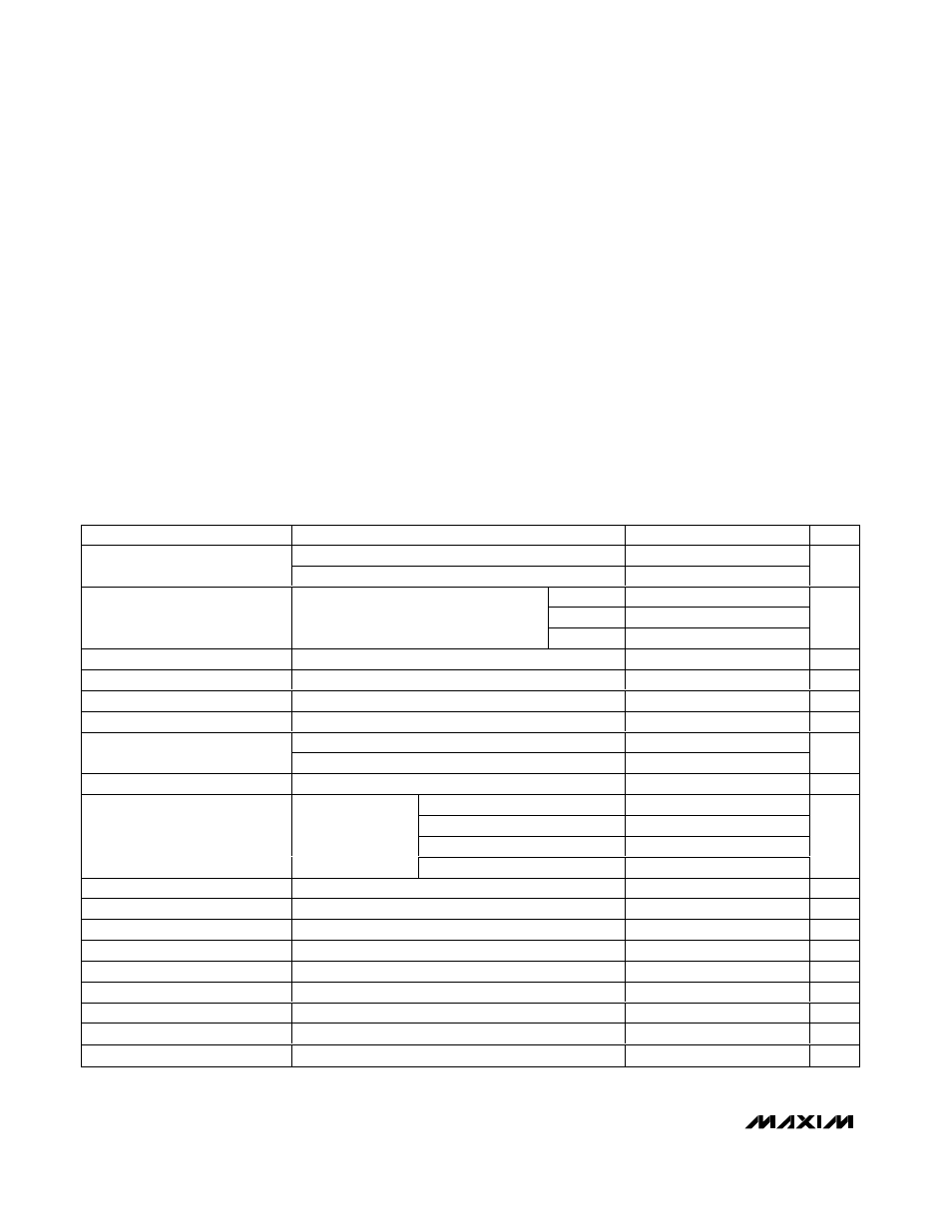
ELECTRICAL CHARACTERISTICS
(Circuit of Figure 1, V+ = 15V, V
CC
= V
DD
= 5V, SKIP = GND,
T
A
= 0
°
C to +85
°
C
, unless otherwise noted. Typical values are at
T
A
= +25
°
C.)
PARAMETER
CONDITIONS
MIN
TYP
MAX
UNITS
Battery voltage, V+
2
28
Input Voltage Range
V
CC
, V
DD
4.5
5.5
V
FB = OUT
0.99
1.01
FB = GND
2.475
2.5
2.525
Error Comparator Threshold
(DC Output Voltage Accuracy)
(Note 1)
V+ = 4.5V to 28V,
SKIP = V
CC
FB = V
CC
1.782
1.8
1.818
V
Load Regulation Error
I
LOAD
= 0 to 3A, SKIP = V
CC
9
mV
Line Regulation Error
V
CC
= 4.5V to 5.5V, V+ = 4.5V to 28V
5
mV
FB Input Bias Current
-0.1
+0.1
µA
Output Adjustment Range
1
5.5
V
FB = GND
90
190
350
OUT Input Resistance
FB = V
CC
or adjustable feedback mode
70
145
270
k
Ω
Soft-Start Ramp Time
Rising edge of SHDN to full current limit
1.7
ms
TON = GND (600kHz)
140
160
180
TON = REF (450kHz)
175
200
225
TON = unconnected (300kHz)
260
290
320
On-Time
V+ = 24V,
V
OUT
= 2V
(Note 2)
TON = V
CC
(200kHz)
380
425
470
ns
Minimum Off-Time
(Note 2)
400
500
ns
Quiescent Supply Current (V
CC
)
FB forced above the regulation point
550
800
µA
Quiescent Supply Current (V
DD
)
FB forced above the regulation point
<1
5
µA
Quiescent Supply Current (V+)
25
40
µA
Shutdown Supply Current (V
CC
)
SHDN = GND
<1
5
µA
Shutdown Supply Current (V
DD
)
SHDN = GND
<1
5
µA
Shutdown Supply Current (V+)
SHDN = GND, V+ = 28V, V
CC
= V
DD
= 0 or 5V
<1
5
µA
Reference Voltage
V
CC
= 4.5V to 5.5V, no external REF load
1.98
2.00
2.02
V
Reference Load Regulation
I
REF
= 0 to 50µA
0.01
V