Rainbow Electronics MAX1712 User Manual
Page 25
MAX1710/MAX1711/MAX1712
High-Speed, Digitally Adjusted
Step-Down Controllers for Notebook CPUs
______________________________________________________________________________________
25
;
;
;
;
;
;
;
;
;
;
;
D1
Q2
V
BATT
GND IN
COUT
VIA TO FB
NEAR COUT+
VIA TO LX
VIA TO SOURCE
OF Q2
VIA TO PGND
NEAR Q2 SOURCE
INDUCTOR DISCHARGE PATH HAS LOW DC RESISTANCE.
VIA TO FBS
VIA TO GNDS
GND
OUT
V
OUT
L1
Q1
CC
V
CC
V
DD
REF
GND
ALL ANALOG GROUNDS
CONNECT TO GND ONLY.
NOTES: "STAR" GROUND IS USED.
D1 IS DIRECTLY ACROSS Q2.
CONNECT GND TO PGND
BENEATH IC, 1 POINT ONLY.
SPLIT ANALOG GND PLANE AS SHOWN.
I
LIM
;
;
;
;
MAX1710
MAX1711
MAX1712
;
;
CIN
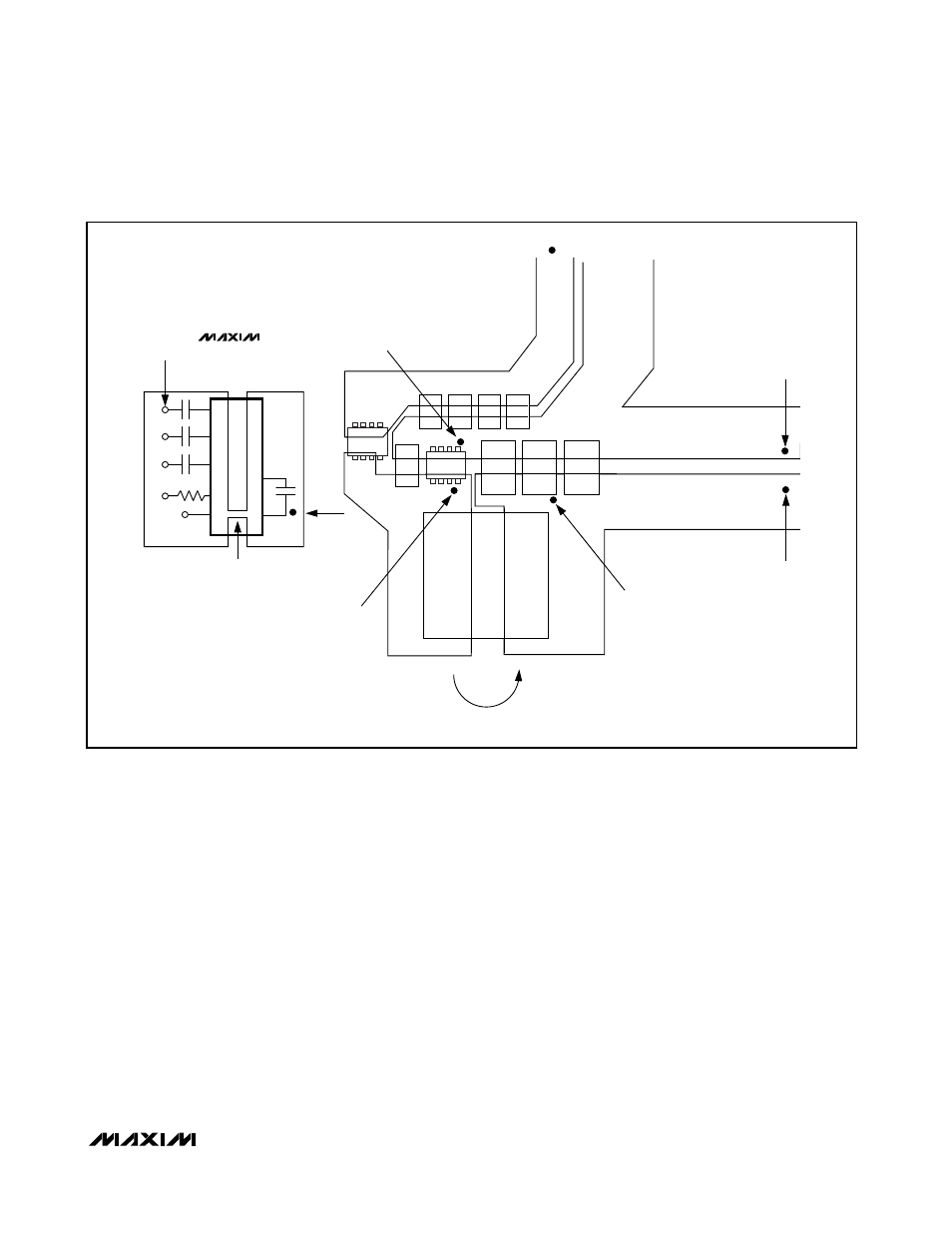
Figure 11. Power-Stage PC Board Layout Example
recovery overshoot, and c) minimize input surge cur-
rents.
The optional 74HC86 exclusive-OR gate detects code
transitions on each of the four most-significant DAC
inputs. The transition detector output goes to a precision
pulse stretcher, a timer that extends the pulse for 75µs
(nominal). This signal then feeds three circuits: the
power-good detector, the SKIP input, and the ILIM cur-
rent-limit control input, thus reducing the current-limit
threshold during the transition interval (in order to reduce
battery current surges). Likewise, SKIP going high
asserts forced PWM mode in order to drag the output
voltage down to the new value. Forced PWM mode is
incompatible with good light-load efficiency due to
inductor-current recirculation losses and gate-drive loss-
es. Therefore, SKIP is driven high only during the 100µs
max transition interval.
The power-good output signal is the logical OR of the
75µs timer signal and the MAX1711/MAX1712 PGOOD
signal. The internal PGOOD detector circuit monitors
only output undervoltage; PGOOD will probably go low
during upward transitions, but not downward. The final
power-good output will always go low for at least 75µs
due to the timer signal.
Load current capability is 15A peak and 12A continuous
over a 10V to 22V input range. All three MOSFETs
require good heatsinking. See the MAX1711 EV kit man-
ual for a complete bill of materials.
PC Board Layout Guidelines
Careful PC board layout is critical to achieving low
switching losses and clean, stable operation. The
switching power stage requires particular attention
(Figure 11). If possible, mount all of the power compo-
nents on the top side of the board with their ground ter-
minals flush against one another. Follow these
guidelines for good PC board layout: