5v bias supply (v, And v – Rainbow Electronics MAX1712 User Manual
Page 10
MAX1710/MAX1711/MAX1712
rent-mode PWMs while also avoiding the problems
caused by widely varying switching frequencies in con-
ventional constant-on-time and constant-off-time PWM
schemes.
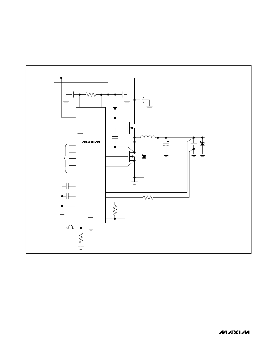
+5V Bias Supply (V
CC
and V
DD
)
The MAX1710/MAX1711/MAX1712 require an external
+5V bias supply in addition to the battery. Typically, this
+5V bias supply is the notebook’s 95% efficient 5V sys-
tem supply. Keeping the bias supply external to the IC
improves efficiency and eliminates the cost associated
with the +5V linear regulator that would otherwise be
needed to supply the PWM circuit and gate drivers. If
stand-alone capability is needed, the +5V supply can be
generated with an external linear regulator such as the
MAX1615.
The battery and +5V bias inputs can be tied together if
the input source is a fixed 4.5V to 5.5V supply. If the +5V
bias supply is powered up prior to the battery supply, the
enable signal (SHDN) must be delayed until the battery
voltage is present in order to ensure startup. The +5V
bias supply must provide V
CC
and gate-drive power, so
the maximum current drawn is:
High-Speed, Digitally Adjusted
Step-Down Controllers for Notebook CPUs
10
______________________________________________________________________________________
V
CC
V
BATT
4.5V TO 28V
+5V
BIAS SUPPLY
C2
3 x 470
µF
KEMET T510
PANASONIC
ETQP6F2R0HFA
POWER-GOOD
INDICATOR
*MAX1710 ONLY
**MAX1711/MAX1712 ONLY
L1
2
µH
V
OUT
1.25V TO 2V AT 7A (MAX1710)
0.925V TO 2V AT 7A (MAX1711)
1.1V TO 1.85V AT 7A (MAX1712)
SHDN
V+
22
1
2
21
20
19
18
17
24
23
13
14
3
4
11
R4
1k
12
7
15
D2
CMPSH-3
C6
1
µF
C7
0.1
µF
C4
1
µF
C3
470pF
TO V
CC
Q1
D1
R2
100k
D3
(OPTIONAL OVP
REVERSE-POLARITY
CLAMP)
Q2
C5
1
µF
R1
20
Ω
C1 3 x 10
µF/30V
SKIP
D0
D1
D2
DAC
INPUTS
ON/OFF
CONTROL
LOW-NOISE
CONTROL
DL
LX
BST
DH
PGND
FB
FBS
GNDS
Q1 = IRF7807
Q2 = IRF7805
D1, D3 = MBRS130T3 (OPTIONAL)
C1 = SANYO OS-CON (30SC10M)
PGOOD
V
DD
MAX1710
MAX1711
MAX1712
8
9
5
6
16
+5V
10
D3
16
D4**
TON
REF
CC
GND
R3
(OPTIONAL)
ILIM
OVP*
Figure 1. Standard Application Circuit