Design procedure – Rainbow Electronics MAX1712 User Manual
Page 17
MAX1710/MAX1711/MAX1712
______________________________________________________________________________________
17
High-Speed, Digitally Adjusted
Step-Down Controllers for Notebook CPUs
open-drain type with no parasitic ESD diodes. Note that
the PGOOD undervoltage detector is completely inde-
pendent of the output UVP fault detector.
Output Overvoltage Protection (OVP)
The OVP circuit is designed to protect against a short-
ed high-side MOSFET by drawing high current and
blowing the battery fuse. The FB node is continuously
monitored for overvoltage. The overvoltage trip thresh-
old tracks the DAC code setting. If the output is more
than 12.5% above the nominal regulation point for
the MAX1710 (2.25V absolute for the MAX1711/
MAX1712), overvoltage protection OVP is triggered and
the circuit shuts down. The DL low-side gate-driver out-
put is then latched high until SHDN is toggled or V
CC
power is cycled below 1V. This action turns on the syn-
chronous-rectifier MOSFET with 100% duty and, in turn,
rapidly discharges the output filter capacitor and forces
the output to ground.
If the condition that caused the overvoltage (such as a
shorted high-side MOSFET) persists, the battery fuse will
blow. Note that DL going high can have the effect of
causing output polarity reversal, due to energy stored in
the output LC at the instant OVP activates. If the load
can’t tolerate being forced to a negative voltage, it may
be desirable to place a power Schottky diode across the
output to act as a reverse-polarity clamp (Figure 1). The
MAX1710/MAX1711/MAX1712 themselves can be
affected by the FB pin going below ground, with the neg-
ative voltage coupling into SHDN. It may be necessary to
add 1k
Ω resistors in series with FB and FBS (Figure 7).
DL is also kept high continuously when V
CC
UVLO is
active as well as in Shutdown1 mode (Table 4).
Overvoltage protection can be defeated via the OVP
input (MAX1710 only) or via a SKIP test mode (see Pin
Description).
Output Undervoltage Protection (UVP)
The output UVP function is similar to foldback current
limiting, but employs a timer rather than a variable cur-
rent limit. If the MAX1710 output (FB) is under 70% of the
nominal value 20ms after coming out of shutdown, the
PWM is latched off and won’t restart until V
CC
power is
cycled or SHDN is toggled. For the MAX1711/MAX1712,
the nominal UVP trip threshold is fixed at 0.8V.
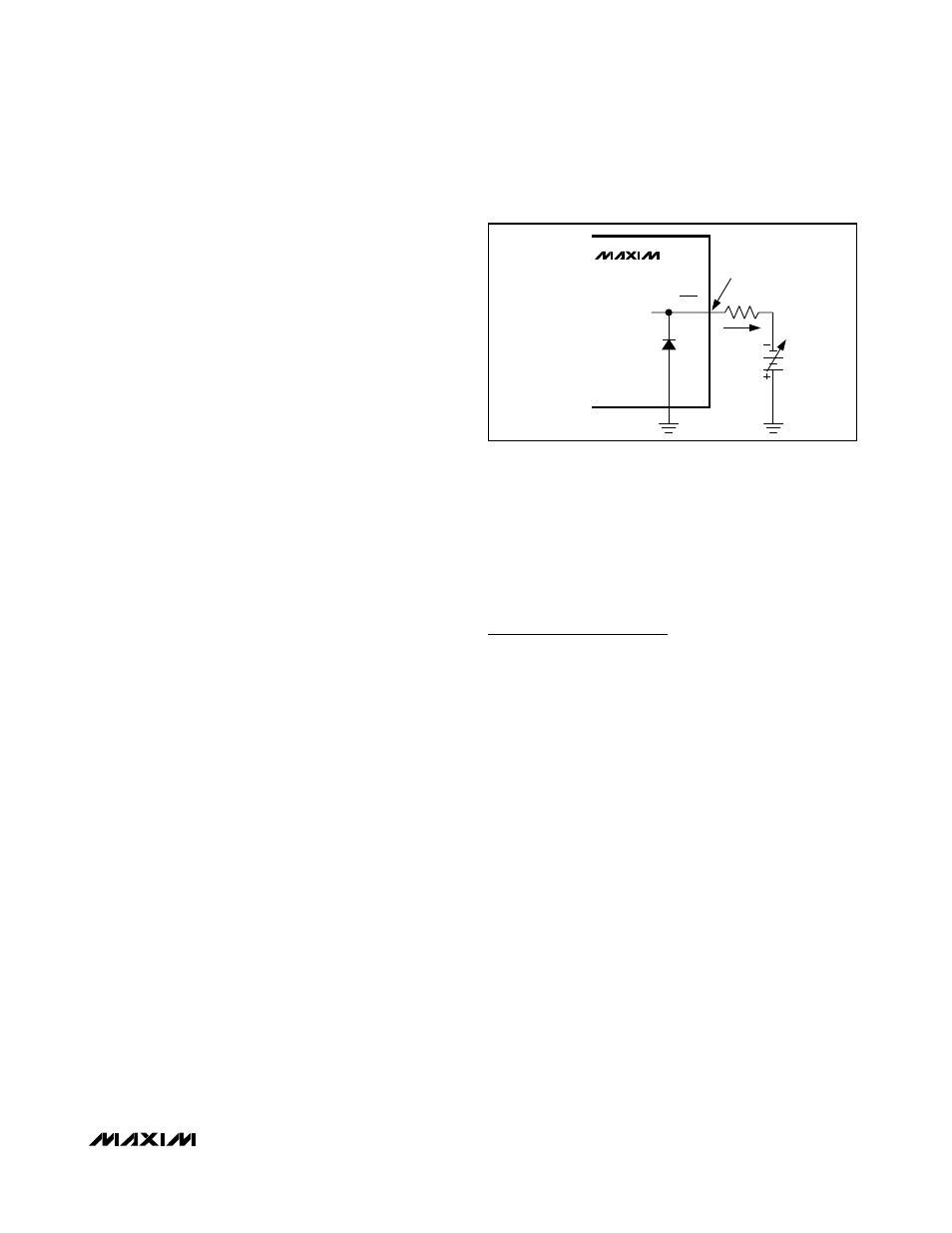
No-Fault Test Mode
The over/undervoltage protection features can compli-
cate the process of debugging prototype breadboards
since there are (at most) a few milliseconds in which to
determine what went wrong. Therefore, a test mode is
provided to totally disable the OVP, UVP, and thermal
shutdown features, and clear to the fault latch if it has
been previously set. The PWM operates as if SKIP were
grounded (PFM/PWM mode).
The no-fault test mode is entered by sinking 1.5mA
from SKIP via an external negative voltage source in
series with a resistor (Figure 6). SKIP is clamped to
GND with a silicon diode, so choose the resistor value
equal to (V
FORCE
- 0.65V) / 1.5mA.
Design Procedure
Firmly establish the input voltage range and maximum
load current before choosing a switching frequency and
inductor operating point (ripple current ratio). The prima-
ry design trade-off lies in choosing a good switching fre-
quency and inductor operating point, and the following
four factors dictate the rest of the design:
1) Input voltage range. The maximum value (V
BATT
(MAX)
) must accommodate the worst-case high AC
adapter voltage. The minimum value (V
BATT(MIN)
)
must account for the lowest battery voltage after
drops due to connectors, fuses, and battery selector
switches. If there is a choice at all, lower input volt-
ages result in better efficiency.
2) Maximum load current. There are two values to con-
sider. The peak load current (I
LOAD(MAX)
) determines
the instantaneous component stresses and filtering
requirements, and thus drives output capacitor
selection, inductor saturation rating, and the design
of the current-limit circuit. The continuous load cur-
rent (I
LOAD
) determines the thermal stresses and
thus drives the selection of input capacitors,
MOSFETs, and other critical heat-contributing com-
ponents. Modern notebook CPUs generally exhibit
I
LOAD
= I
LOAD(MAX)
✕
80%.
3) Switching frequency. This choice determines the
basic trade-off between size and efficiency. The opti-
mal frequency is largely a function of maximum input
APPROXIMATELY
-0.65V
1.5mA
V
FORCE
SKIP
GND
MAX1710
MAX1711
MAX1712
Figure 6. Disabling Over/Undervoltage Protection (Test Mode)