Table 6. approximate k-factors errors – Rainbow Electronics MAX1712 User Manual
Page 20
input voltage don’t exceed the package ratings or violate
the overall thermal budget.
Choose a low-side MOSFET (Q2) that has the lowest
possible R
DS(ON)
, comes in a moderate to small pack-
age (i.e., SO-8), and is reasonably priced. Ensure that
the MAX1710/MAX1711/MAX1712 DL gate driver can
drive Q2; in other words, check that the gate isn’t pulled
up by the high-side switch turning on due to parasitic
drain-to-gate capacitance, causing cross-conduction
problems. Switching losses aren’t an issue for the low-
side MOSFET since it’s a zero-voltage switched device
when used in the buck topology.
MOSFET Power Dissipation
Worst-case conduction losses occur at the duty factor
extremes. For the high-side MOSFET, the worst-case
power dissipation due to resistance occurs at minimum
battery voltage:
PD(Q1) = (V
OUT
/ V
BATT(MIN)
)
✕
I
LOAD
2
✕
R
DS(ON)
Generally, a small high-side MOSFET is desired in order
to reduce switching losses at high input voltages.
However, the R
DS(ON)
required to stay within package
power-dissipation limits often limits how small the MOS-
FET can be. Again, the optimum occurs when the switch-
ing (AC) losses equal the conduction (R
DS(ON)
) losses.
High-side switching losses don’t usually become an
issue until the input is greater than approximately 15V.
Switching losses in the high-side MOSFET can become
an insidious heat problem when maximum AC adapter
voltages are applied, due to the squared term in the
CV
2
F switching loss equation. If the high-side MOSFET
you’ve chosen for adequate R
DS(ON)
at low battery volt-
ages becomes extraordinarily hot when subjected to
V
BATT(MAX)
, you must reconsider your choice of MOS-
FET.
Calculating the power dissipation in Q1 due to switching
losses is difficult, since it must allow for difficult-to-quanti-
MAX1710/MAX1711/MAX1712
High-Speed, Digitally Adjusted
Step-Down Controllers for Notebook CPUs
20
______________________________________________________________________________________
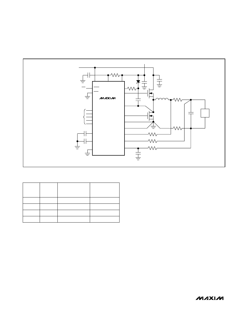
V+
V
CC
V
IN
= 7V TO 24V*
SHDN
SKIP
REF
DAC
INPUTS
ON/OFF
CC
0.22
µF
470pF
DL
D0
LX
BST
5
Ω
DH
PGND
GND
FB
Q1
+5V
20
Ω
0.1
µF
1
µF
Q2
0.5
µH
0.1
µF
1nF
C1
1k
R1
C2
CPU
1.6V AT 7A
1k
1k
V
DD
FBS
GNDS
MAX1711
MAX1712
R2
C1 = 4 x 4.7
µF/25V TAIYO YUDEN (TMK325BJ475K)
C2 = 6 x 47
µF/10V TAIYO YUDEN (LMK550BJ476KM)
R1 + R2 = 5m
Ω MINIMUM OF PC BOARD TRACE RESISTANCE (TOTAL)
D1
D2
D3
D4
TON
*FOR HIGHER MINIMUM INPUT VOLTAGE,
*
LESS OUTPUT CAPACITANCE IS REQUIRED.
Figure 7. All-Ceramic-Capacitor Application
TON
SETTING
(kHz)
APPROXIMATE
K-FACTOR
ERROR (%)
MIN V
BATT
AT V
OUT
= 2V
(V)
200
±10
2.6
300
±10
2.9
400
±12.5
3.2
550
±12.5
3.6
K
FACTOR
(µs-V)
5
3.3
2.5
1.8
Table 6. Approximate K-Factors Errors