Electrical characteristics (continued) – Rainbow Electronics MAX1715 User Manual
Page 3
MAX1715
Ultra-High Efficiency, Dual Step-Down
Controller for Notebook Computers
_______________________________________________________________________________________
3
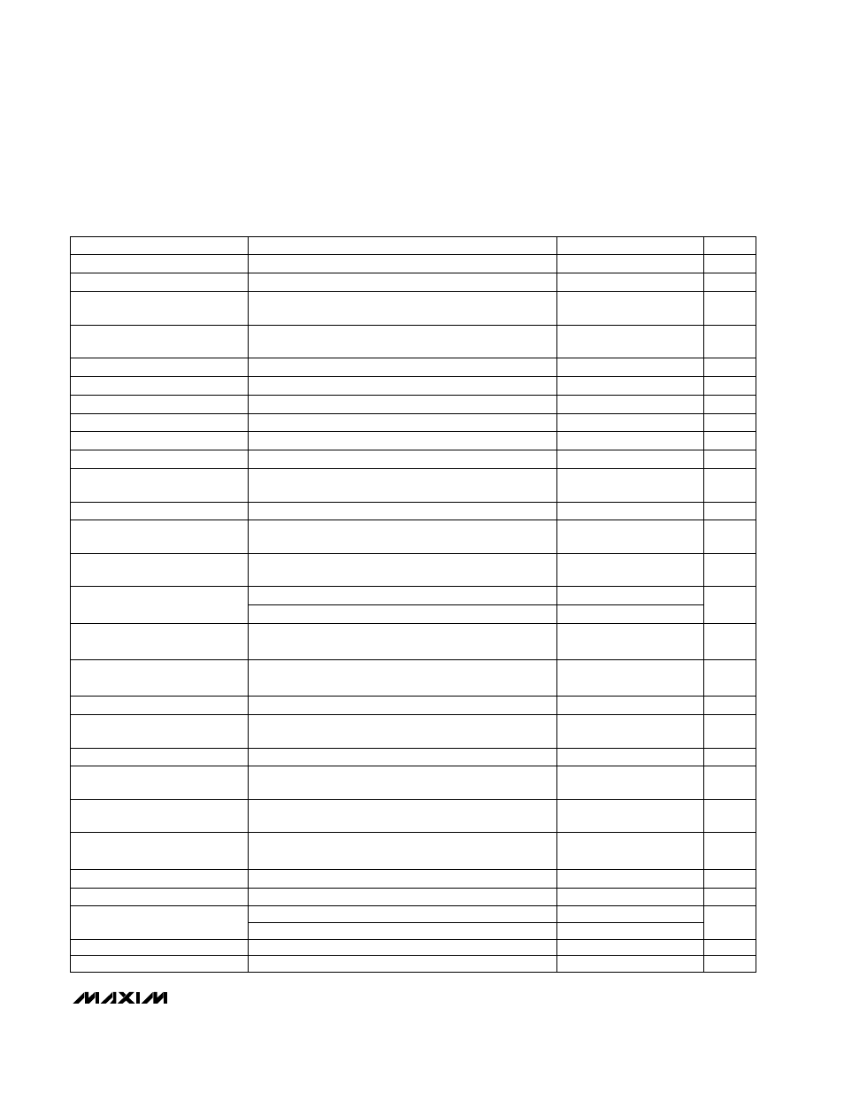
ELECTRICAL CHARACTERISTICS (continued)
(Circuit of Figure 1, 4A components from Table 1, V
CC =
V
DD
= +5V, SKIP = AGND, V+ = 15V, T
A
= 0°C to +85°C, unless otherwise
noted.) (Note 1)
(Note 3)
ns
400
500
Minimum Off-Time
I
REF
= 0 to 50µA
No external REF load
ON1 = ON2 = 0
V
2
0.01
Reference Load Regulation
V
1.98
2
2.02
Reference Voltage
µA
<1
5
Shutdown Supply Current (V+)
µA
<1
5
Shutdown Supply Current
(V
CC
+ V
DD
)
Falling edge, hysteresis = 40mV
V
1.6
REF Fault Lockout Voltage
10
PGND - LX_, I
LIM
resistor = 100k
Ω
mV
40
50
60
Current-Limit Threshold
(Positive Direction, Adjusted)
PGND - LX_, T
A
= +25°C, I
LIM
= V
CC
mV
-145
-120
-95
Current-Limit Threshold
(Negative Direction)
PGND - LX_, SKIP = AGND
mV
-5
3
10
Current-Limit Threshold, Zero
Crossing
Hysteresis = 10°C
°C
150
Thermal Shutdown Threshold
Rising edge, hysteresis = 20mV, PWM disabled below
this level
V
4.1
4.4
V
CC
Undervoltage Lockout
Threshold
BST - LX forced to 5V
Ω
1.5
5
DH Gate Driver On-Resistance
FB1 and FB2 forced above the regulation point
µA
1100
1600
Quiescent Supply Current
(V
CC
+ V
DD
)
µA
25
70
Quiescent Battery Current (V+)
FB_ forced 2% above trip threshold
µs
1.5
Overvoltage Fault Propagation
Delay
With respect to error comparator threshold
%
8.5
10.5
13
Overvoltage Trip Threshold
With respect to error comparator threshold
%
60
70
80
Output Undervoltage Threshold
From ON_ signal going high
ms
10
20
30
Output Undervoltage Lockout
Time
PGND - LX_, I
LIM
= V
CC
mV
75
100
125
Current-Limit Threshold
(Positive Direction, Fixed)
ON1 = ON2 = 0
DL, high state
Ω
1.5
5
DL Gate Driver On-Resistance
(pull-up)
0.6
2.5
A
DH Gate Driver Source/Sink
Current
DH forced to 2.5V, BST_ - LX_ forced to 5V
1
A
DL Gate Driver Source Current
DL forced to 2.5V
1
A
DL Gate Driver Sink Current
DL forced to 2.5V
3
ns
Dead Time
DL rising
35
REF in regulation
REF Sink Current
DL, low state
DL Gate Driver On-Resistance
(pull-down)
Ω
µA
CONDITIONS
UNITS
MIN
TYP
MAX
PARAMETER
PGND - LX_, I
LIM
resistor = 400k
Ω
160
200
240
DH rising
26
ON_, SKIP
0.8
V
Logic Input High Voltage
ON_, SKIP
2.4
V
Logic Input Low Voltage