Pc board layout guidelines – Rainbow Electronics MAX1715 User Manual
Page 22
MAX1715
Ultra-High Efficiency, Dual Step-Down
Controller for Notebook Computers
22
______________________________________________________________________________________
switching frequency and a much smaller inductor
value.
PC Board Layout Guidelines
Careful PC board layout is critical to achieving low
switching losses and clean, stable operation. This is
especially true for dual converters, where one channel
can affect the other. The switching power stages require
particular attention (Figure 11). Refer to the MAX1715
EV kit data sheet for a specific layout example.
If possible, mount all of the power components on the
top side of the board with their ground terminals flush
against one another. Follow these guidelines for good
PC board layout:
• Isolate the power components on the top side from
the sensitive analog components on the bottom side
with a ground shield. Use a separate PGND plane
under the OUT1 and OUT2 sides (called PGND1 and
PGND2). Avoid the introduction of AC currents into
the PGND1 and PGND2 ground planes. Run the
power plane ground currents on the top side only, if
possible.
• Use a star ground connection on the power plane to
minimize the crosstalk between OUT1 and OUT2.
• Keep the high-current paths short, especially at the
ground terminals. This practice is essential for sta-
ble, jitter-free operation.
• Tie AGND and PGND together close to the IC. Do
not connect them together anywhere else. Carefully
follow the grounding instructions under Step 4 of the
Layout Procedure.
• Keep the power traces and load connections short.
This practice is essential for high efficiency. Using
thick copper PC boards (2oz vs. 1oz) can enhance
full-load efficiency by 1% or more. Correctly routing
PC board traces is a difficult task that must be
approached in terms of fractions of centimeters,
where a single milliohm of excess trace resistance
causes a measurable efficiency penalty.
• LX_ and PGND connections to the synchronous rec-
tifiers for current limiting must be made using Kelvin
sense connections to guarantee the current-limit
accuracy. With SO-8 MOSFETs, this is best done by
routing power to the MOSFETs from outside using
the top copper layer, while tying in PGND and LX_
inside (underneath) the SO-8 package.
• When trade-offs in trace lengths must be made, it’s
preferable to allow the inductor charging path to be
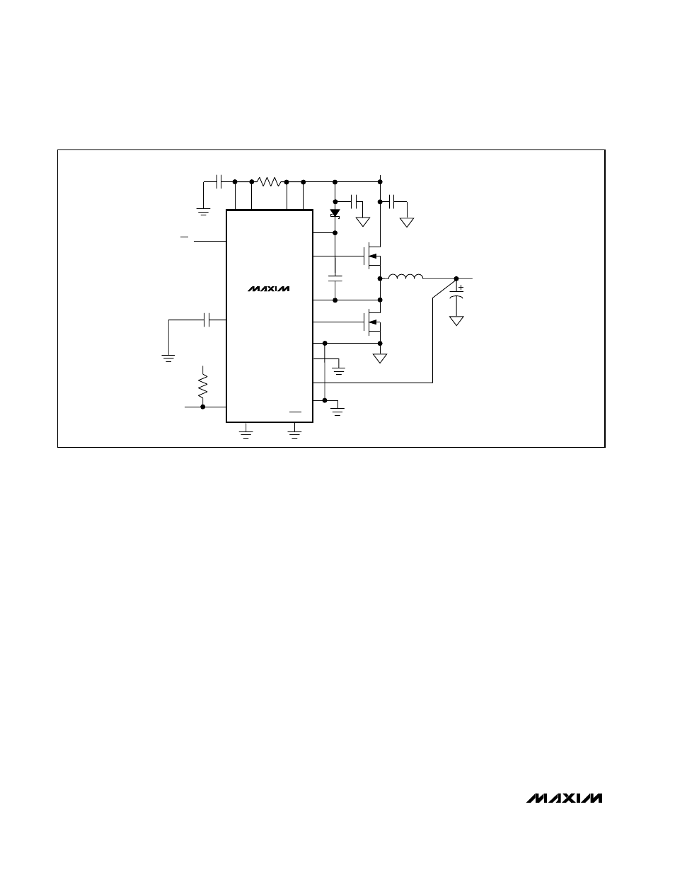
ILIM V
CC
V
IN
4.5V TO 5.5V
L1
0.5
µH
V
OUT
2.5V AT 7A
ON2
1
µF
0.1
µF
0.22
µF
C2
3 x 470
µF
KEMET T510
IRF7805
IRF7805
1
µF
20
Ω
C1
4 x 10
µF/25V
ON/OFF
DL2
LX2
BST2
DH2
PGND
OUT2
FB2
AGND
V
DD
V
CC
V+
MAX1715
REF
TON
SKIP
100k
PGOOD
Figure 10. 5V-Powered, 8A CPU Buck Regulator