Design procedure – Rainbow Electronics MAX1715 User Manual
Page 17
MAX1715
Ultra-High Efficiency, Dual Step-Down
Controller for Notebook Computers
______________________________________________________________________________________
17
Overvoltage protection can be defeated through the
SKIP test mode (Table 3).
Output Undervoltage Protection (UVP)
The output undervoltage protection function is similar to
foldback current limiting, but employs a timer rather
than a variable current limit. If the MAX1715 output volt-
age is under 70% of the nominal value 20ms after com-
ing out of shutdown, the PWM is latched off and won’t
restart until V
CC
power is cycled or SHDN is toggled.
No-Fault Test Mode
The over/undervoltage protection features can compli-
cate the process of debugging prototype breadboards
since there are (at most) a few milliseconds in which to
determine what went wrong. Therefore, a test mode is
provided to totally disable the OVP, UVP, and thermal
shutdown features, and clear the fault latch if it has
been set. The PWM operates as if SKIP were grounded
(PFM/PWM mode).
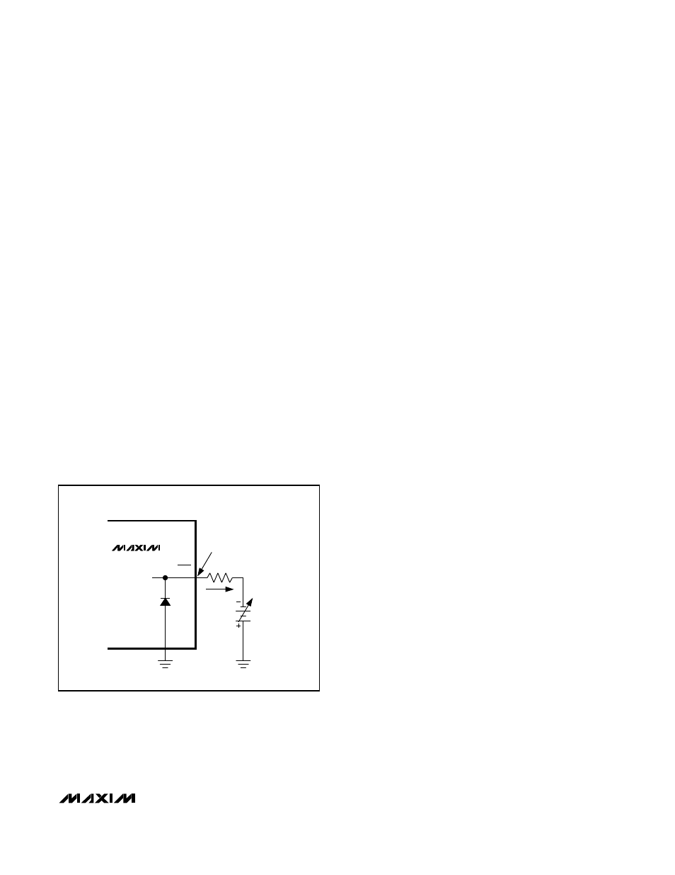
The no-fault test mode is entered by sinking 1.5mA
from SKIP through an external negative voltage source
in series with a resistor (Figure 7). SKIP is clamped to
AGND with a silicon diode, so choose the resistor value
equal to (V
FORCE
- 0.65V) / 1.5mA.
__________________Design Procedure
Firmly establish the input voltage range and maximum
load current before choosing a switching frequency
and inductor operating point (ripple-current ratio). The
primary design trade-off lies in choosing a good switch-
ing frequency and inductor operating point, and the fol-
lowing four factors dictate the rest of the design:
1) Input voltage range. The maximum value (V
IN(MAX)
)
must accommodate the worst-case high AC adapter
voltage. The minimum value (V
IN(MIN)
) must account
for the lowest battery voltage after drops due to con-
nectors, fuses, and battery selector switches. If
there is a choice at all, lower input voltages result in
better efficiency.
2) Maximum load current. There are two values to
consider. The peak load current (I
LOAD(MAX)
) deter-
mines the instantaneous component stresses and fil-
tering requirements, and thus drives output
capacitor selection, inductor saturation rating, and
the design of the current-limit circuit. The continuous
load current (I
LOAD
) determines the thermal stresses
and thus drives the selection of input capacitors,
MOSFETs, and other critical heat-contributing com-
ponents. Modern notebook CPUs generally exhibit
I
LOAD
= I
LOAD(MAX)
· 80%.
3) Switching frequency. This choice determines the
basic trade-off between size and efficiency. The
optimal frequency is largely a function of maximum
input voltage, due to MOSFET switching losses that
are proportional to frequency and V
IN
2. The opti-
mum frequency is also a moving target, due to rapid
improvements in MOSFET technology that are mak-
ing higher frequencies more practical (Table 4).
4) Inductor operating point. This choice provides
trade-offs between size vs. efficiency. Low inductor
values cause large ripple currents, resulting in the
smallest size, but poor efficiency and high output
noise. The minimum practical inductor value is one
that causes the circuit to operate at the edge of criti-
cal conduction (where the inductor current just
touches zero with every cycle at maximum load).
Inductor values lower than this grant no further size-
reduction benefit.
The MAX1715’s pulse-skipping algorithm initiates
skip mode at the critical conduction point. So, the
inductor operating point also determines the load-
current value at which PFM/PWM switchover occurs.
The optimum point is usually found between 20%
and 50% ripple current.
APPROXIMATELY
-0.65V
1.5mA
V
FORCE
SKIP
AGND
MAX1715
Figure 7. Disabling Over/Undervoltage Protection (Test Mode)