Rainbow Electronics MAX1715 User Manual
Page 23
MAX1715
Ultra-High Efficiency, Dual Step-Down
Controller for Notebook Computers
______________________________________________________________________________________
23
made longer than the discharge path. For example,
it’s better to allow some extra distance between the
input capacitors and the high-side MOSFET than to
allow distance between the inductor and the low-
side MOSFET or between the inductor and the out-
put filter capacitor.
• Ensure that the OUT connection to C
OUT
is short and
direct. However, in some cases it may be desirable
to deliberately introduce some trace length between
the OUT inductor node and the output filter capacitor
(see the All-Ceramic-Capacitor Application section).
• Route high-speed switching nodes (BST_, LX_, DH_,
and DL_) away from sensitive analog areas (REF,
ILIM, FB). Use PGND1 and PGND2 as EMI shields to
keep radiated switching noise away from the IC,
feedback dividers, and analog bypass capacitors.
• Make all pin-strap control input connections (SKIP,
ILIM, etc.) to AGND or V
CC
rather than PGND_or
V
DD
.
Layout Procedure
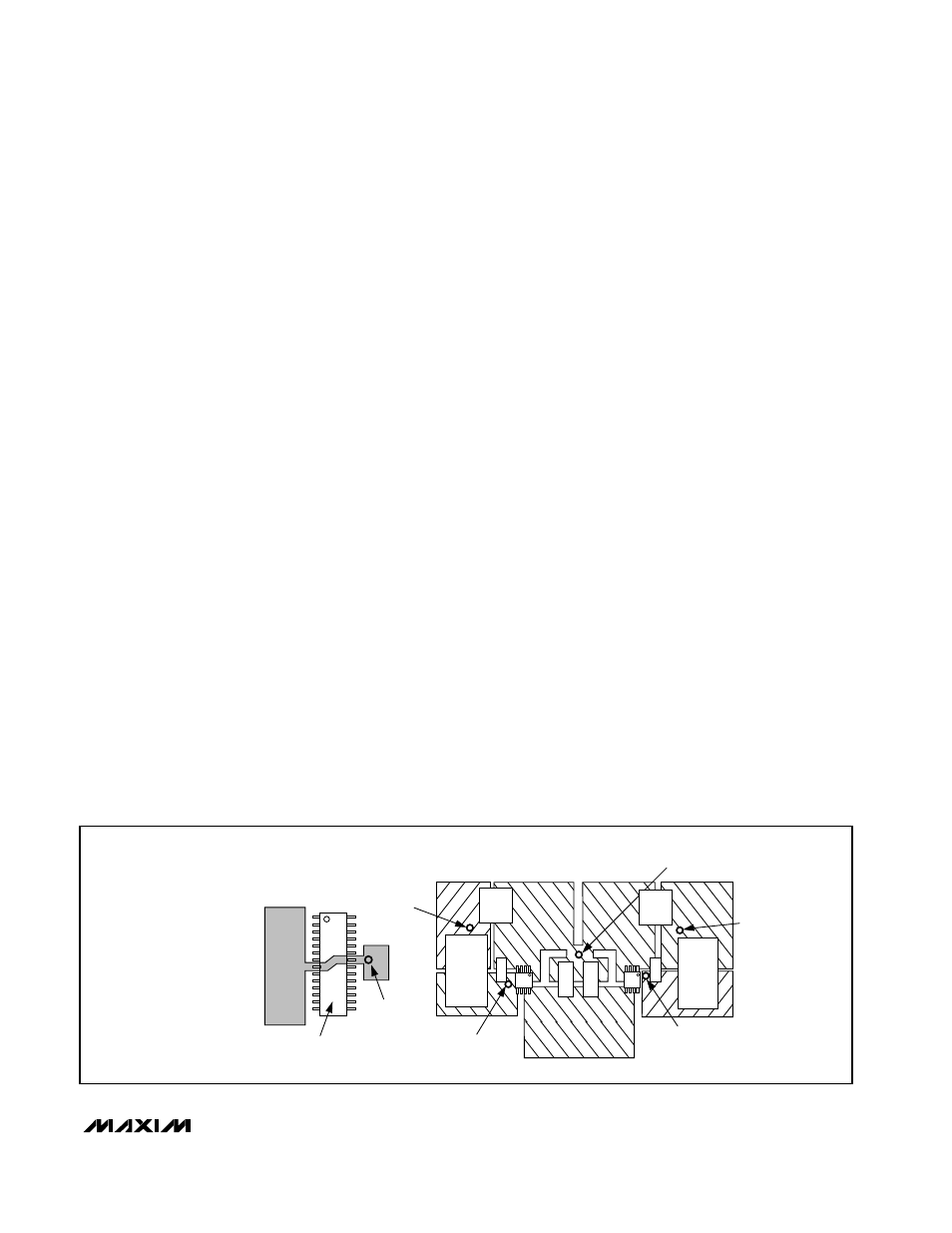
1) Place the power components first, with ground termi-
nals adjacent (Q2 source, C
IN
-, C
OUT
-, D1 anode). If
possible, make all these connections on the top
layer with wide, copper-filled areas.
2) Mount the controller IC adjacent to the synchronous
rectifiers MOSFETs, preferably on the back side in
order to keep LX_, PGND_, and the DL_ gate-drive
line short and wide. The DL_ gate trace must be
short and wide, measuring 10 to 20 squares (50mils
to 100mils wide if the MOSFET is 1 inch from the
controller IC).
3) Group the gate-drive components (BST_ diode and
capacitor, V
DD
bypass capacitor) together near the
controller IC.
4) Make the DC-DC controller ground connections as
follows: near the IC, create a small analog ground
plane. Connect this plane to AGND and use this
plane for the ground connection for the REF and
V
CC
bypass capacitors, FB dividers, and I
LIM
resis-
tors (if any). Create another small ground island for
PGND, and use it for the V
DD
bypass capacitor,
placed very close to the IC. Connect the AGND and
the PGND pins together under the IC (this is the only
connection between AGND and PGND).
5) On the board’s top side (power planes), make a star
ground to minimize crosstalk between the two sides.
The top-side star ground is a star connection of the
input capacitors, side 1 low-side MOSFET, and side
2 low-side MOSFET. Keep the resistance low
between the star ground and the source of the low-
side MOSFETs for accurate current limit. Connect
the top-side star ground (used for MOSFET, input,
and output capacitors) to the small PGND island with
a short, wide connection (preferably just a via).
If multiple layers are available (highly recommend-
ed), create PGND1 and PGND2 islands on the layer
just below the top-side layer (refer to the MAX1715
EV kit for an example) to act as an EMI shield.
Connect each of these individually to the star ground
via, which connects the top side to the PGND plane.
Add one more solid ground plane under the IC to act
as an additional shield, and also connect that to the
star ground via.
6) Connect the output power planes (V
CORE
and sys-
tem ground planes) directly to the output filter
capacitor positive and negative terminals with multi-
ple vias.
AGND
PGND
VIA TO OUT1
GROUND
OUT2
OUT1
VIA TO OUT2
VIA TO PGND
VIA TO LX1
V
IN
VIA TO LX2
USE AGND PLANE TO:
- BYPASS V
CC
AND REF
- TERMINATE EXTERNAL FB
DIVIDER (IF USED)
- TERMINATE R
ILIM
(IF USED)
- PIN-STRAP CONTROL
INPUTS
USE PGND PLANE TO:
- BYPASS V
DD
- CONNECT PGND TO THE TOPSIDE STAR GROUND
VIA TO GROUND
NOTE: EXAMPLE SHOWN IS FOR DUAL N-CHANNEL MOSFET.
CONNECT PGND TO AGND
BENEATH THE MAX1715 AT
ONE POINT ONLY AS SHOWN.
C4
C3
C1
N1
D1
D2
N2
C2
L1
L2
Figure 11. PC Board Layout Example