Timing characteristics—max1083 – Rainbow Electronics MAX1083 User Manual
Page 7
MAX1082/MAX1083
300ksps/400ksps, Single-Supply, 4-Channel,
Serial 10-Bit ADCs with Internal Reference
_______________________________________________________________________________________
7
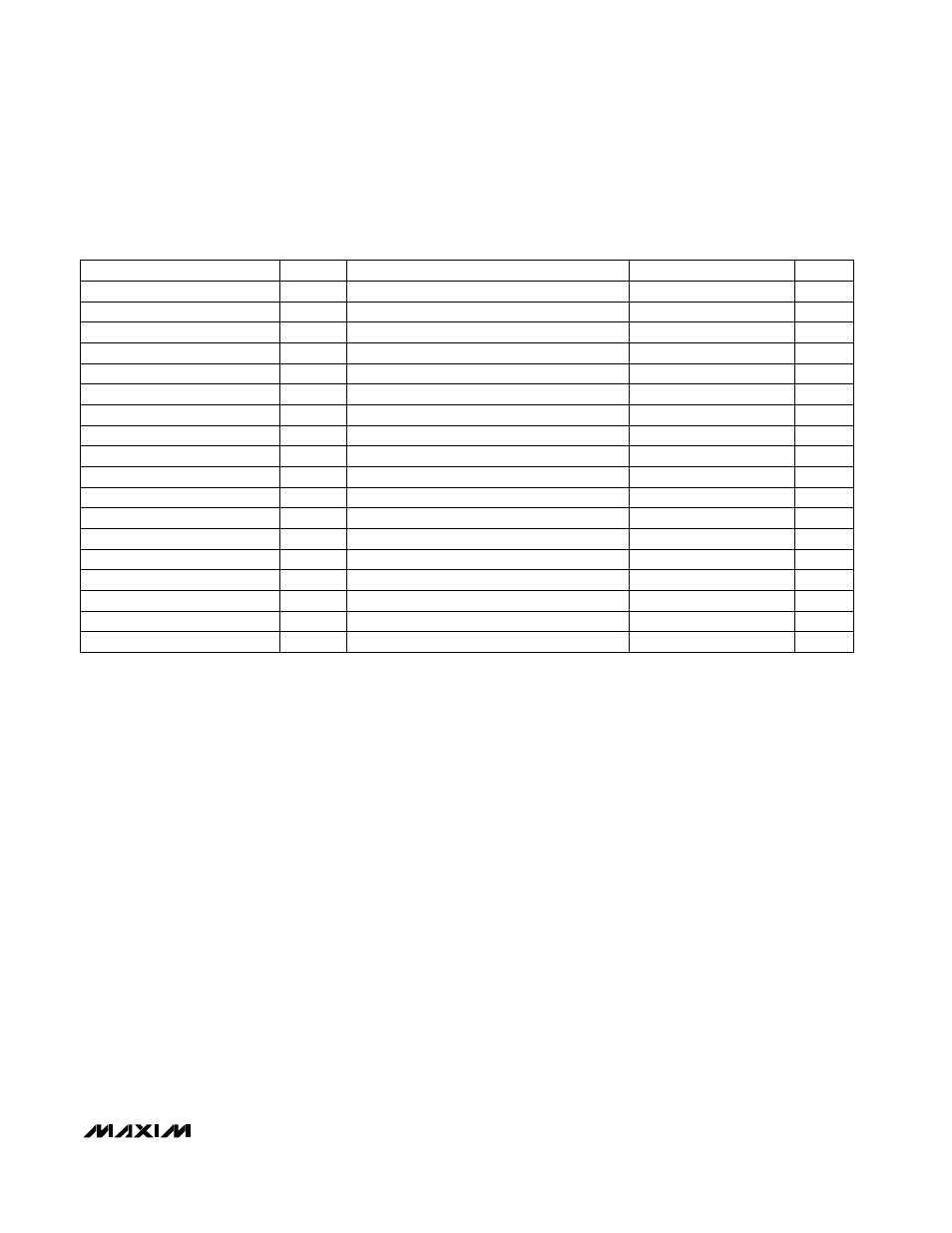
TIMING CHARACTERISTICS—MAX1083
(Figures 1, 2, 5, 6; V
DD1
= V
DD2
= +2.7V to +3.6V; T
A
= T
MIN
to T
MAX
; unless otherwise noted.)
C
LOAD
= 20pF
C
LOAD
= 20pF
C
LOAD
= 20pF
C
LOAD
= 20pF
C
LOAD
= 20pF
C
LOAD
= 20pF
C
LOAD
= 20pF
C
LOAD
= 20pF
CONDITIONS
ns
100
t
CSW
CS Pulse Width High
ns
85
t
STE
CS Fall to SSTRB Enable
ns
85
t
DOE
CS Fall to DOUT Enable
ns
13
85
t
STD
CS Rise to SSTRB Disable
ns
13
85
t
DOD
CS Rise to DOUT Disable
ns
100
t
STV
SCLK Rise to SSTRB Valid
ns
100
t
DOV
SCLK Rise to DOUT Valid
ns
83
t
CL
SCLK Pulse Width Low
ns
83
t
CH
ns
208
t
CP
SCLK Period
SCLK Pulse Width High
ns
13
20
t
STH
SCLK Rise to SSTRB Hold
ns
13
20
t
DOH
SCLK Rise to DOUT Hold
ns
45
t
CS1
CS Rise to SCLK Rise Ignore
ns
45
t
CSO
SCLK Rise to CS Fall ignore
ns
45
t
DS
DIN to SCLK Setup
ns
0
t
DH
DIN to SCLK Hold
ns
45
t
CSS
CS Fall to SCLK Rise Setup
ns
0
t
CSH
SCLK Rise to CS Rise Hold
UNITS
MIN
TYP
MAX
SYMBOL
PARAMETER
Note 1: Tested at V
DD1
= V
DD2
= V
DD(MIN)
; COM = GND, unipolar single-ended input mode.
Note 2: Relative accuracy is the deviation of the analog value at any code from its theoretical value after the full-scale range has
been calibrated.
Note 3: Offset nulled.
Note 4: Ground the “on” channel; sine wave is applied to all “off” channels.
Note 5: Conversion time is defined as the number of clock cycles multiplied by the clock period; clock has 50% duty cycle.
Note 6: The common-mode range for the analog inputs (CH3–CH0 and COM) is from GND to V
DD1
.
Note 7: External load should not change during conversion for specified accuracy.
Note 8: ADC performance is limited by the converter’s noise floor, typically 300µVp-p. An external reference below 2.5V
compromises the performance of the ADC.
Note 9: Electrical characteristics are guaranteed from V
DD1(MIN)
= V
DD2(MIN)
to V
DD1(MAX)
= V
DD2(MAX)
. For operations beyond
this range, see Typical Operating Characteristics. For guaranteed specifications beyond the limits, contact the factory.
Note 10: AIN = midscale.Unipolar Mode. MAX1082 tested with 20pF on DOUT, 20pF on SSTRB, and f
SCLK
= 6.4MHz, 0 to 5V.
MAX1083 tested with same loads, f
SCLK
= 4.8MHz, 0 to 3V.
Note 11: SCLK = DIN = GND. CS = V
DD1.