Rainbow Electronics MAX1083 User Manual
Page 18
MAX1082/MAX1083
300ksps/400ksps, Single-Supply, 4-Channel,
Serial 10-Bit ADCs with Internal Reference
18
______________________________________________________________________________________
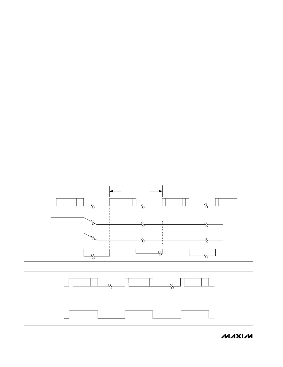
Figure 11a. Full Power-Down Timing
REFADJ
1.22V
1.22V
0V
2.5mA
2.5mA
1.3mA OR 0.9mA
DIN
IV
DD1
+ IV
DD2
REF
FULLPD
REDP
WAIT 1.2ms (7 x RC)
FULLPD
1
0 0
1
1
γ = RC = 17kΩ x 0.01µF
DUMMY CONVERSION
1
1 0
0 0
2.5V
2.5mA
0mA
0mA
2.5V
0V
Figure 11b. FASTPD and REDP Timing
2.5V (ALWAYS ON)
2.5mA
2.5mA
DIN
IV
DD1
+ IV
DD2
REF
REDP
REDP
FASTPD
1
1 0
1
1
1 0
0 1
2.5mA
0.9mA
0.9mA
1.3mA
unipolar operation, and 1LSB = 2.44mV [(2.500V / 2) /
1024] for bipolar operation.
Layout, Grounding, and Bypassing
For best performance, use printed circuit (PC) boards;
wire-wrap boards are not recommended. Board layout
should ensure that digital and analog signal lines are
separated from each other. Do not run analog and digi-
tal (especially clock) lines parallel to one another, or
digital lines underneath the ADC package.
Figure 15 shows the recommended system ground
connections. Establish a single-point analog ground
(star ground point) at GND. Connect all other analog
grounds to the star ground. Connect the digital system
ground to this ground only at this point. For lowest-
noise operation, the ground return to the star ground’s
power supply should be low impedance and as short
as possible.
High-frequency noise in the V
DD1
power supply may
affect the high-speed comparator in the ADC. Bypass
the supply to the star ground with 0.1µF and 10µF
capacitors close to V
DD1
of the MAX1082/MAX1083.
Minimize capacitor lead lengths for best supply-noise
rejection. If the power supply is very noisy, a 10
Ω resis-
tor can be connected as a lowpass filter (Figure 15).
High-Speed Digital Interfacing with QSPI
The MAX1082/MAX1083 can interface with QSPI using
the circuit in Figure 16 (CPOL = 0, CPHA = 0). This QSPI
circuit can be programmed to do a conversion on each of
the four channels. The result is stored in memory without
taxing the CPU, since QSPI incorporates its own microse-
quencer.
TMS320LC3x Interface
Figure 17 shows an application circuit to interface the
MAX1082/MAX1083 to the TMS320 in external clock
mode. The timing diagram for this interface circuit is
shown in Figure 18.
Use the following steps to initiate a conversion in the
MAX1082/MAX1083 and to read the results:
1) The TMS320 should be configured with CLKX
(transmit clock) as an active-high output clock and