Electrical characteristics—max1083 (continued) – Rainbow Electronics MAX1083 User Manual
Page 5
MAX1082/MAX1083
300ksps/400ksps, Single-Supply, 4-Channel,
Serial 10-Bit ADCs with Internal Reference
_______________________________________________________________________________________
5
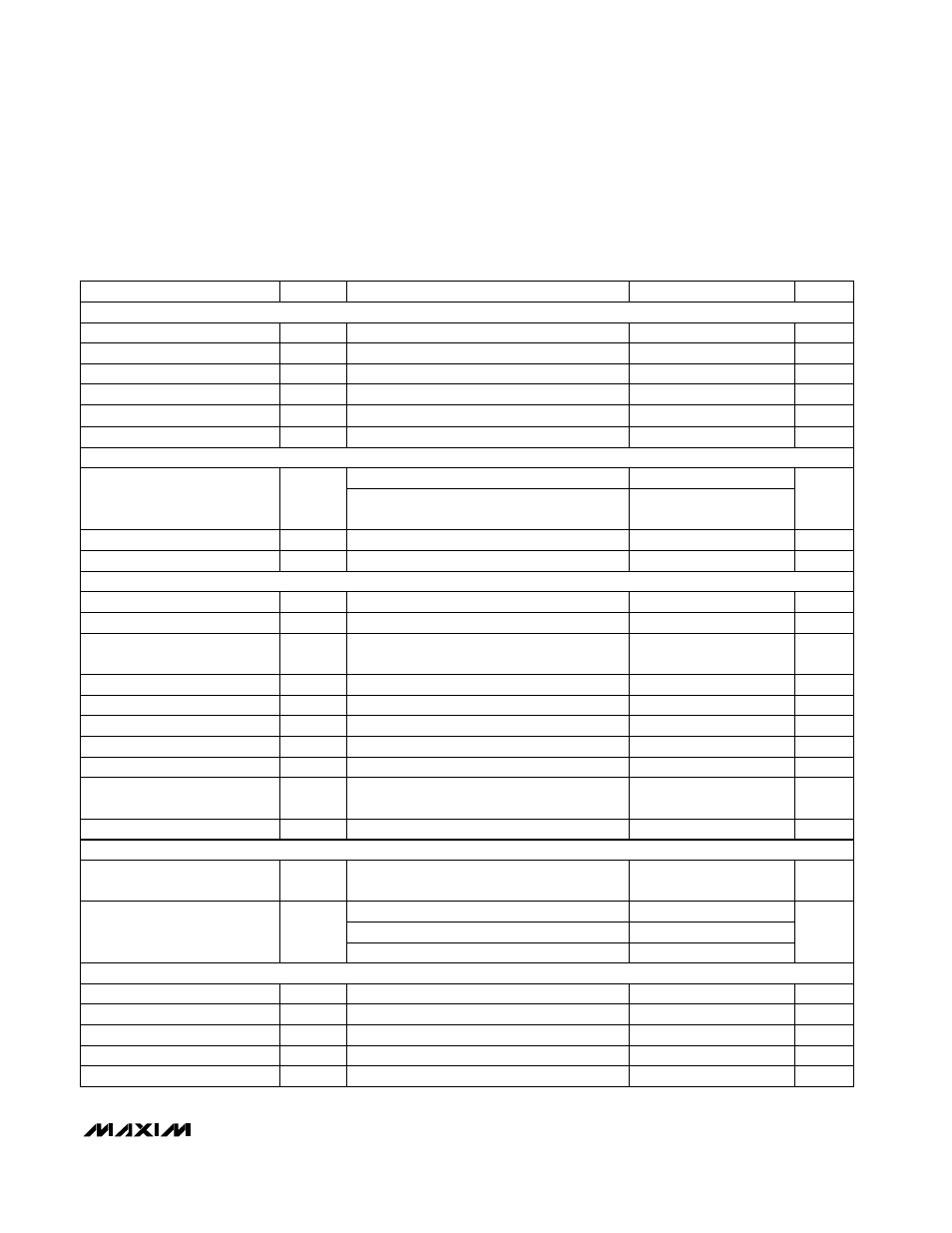
ELECTRICAL CHARACTERISTICS—MAX1083 (continued)
(V
DD1
= V
DD2
= +2.7V to +3.6V, COM = GND, f
OSC
= 4.8MHz, 50% duty cycle, 16 clocks/conversion cycle (300ksps), external
+2.5V at REF, REFADJ = V
DD1
, T
A
= T
MIN
to T
MAX
, unless otherwise noted. Typical values are at T
A
= +25°C.)
Normal operating mode
Normal operating mode
Normal operating mode
CONDITIONS
MHz
0.5
4.8
f
SCLK
Serial Clock Frequency
ps
<50
Aperture Jitter
ns
10
Aperture Delay
ns
625
t
ACQ
Track/Hold Acquisition Time
µs
3.3
t
CONV
Conversion Time (Note 5)
UNITS
MIN
TYP
MAX
SYMBOL
PARAMETER
To power down the internal reference
For small adjustments, from 1.22V
0 to 0.75mA output load
On/off leakage current, V
CH_
= 0 or V
DD1
T
A
= +25°C
Bipolar, V
COM
or V
CH_
= V
REF
/2,
referenced to COM or CH_
Unipolar, V
COM
= 0
V/V
2.05
Buffer Voltage Gain
V
1.4
V
DD1
- 1
REFADJ Buffer Disable
Threshold
mV
±100
REFADJ Input Range
V
1.22
REFADJ Output Voltage
µF
0.01
10
Capacitive Bypass at REFADJ
µF
4.7
10
Capacitive Bypass at REF
mV/mA
0.1
2.0
Load Regulation (Note 7)
ppm/°C
±15
TC V
REF
REF Output Temperature
Coefficient
mA
15
REF Short-Circuit Current
V
2.480
2.500
2.520
V
REF
REF Output Voltage
pF
18
Input Capacitance
µA
±0.001
±1
Multiplexer Leakage Current
±V
REF
/2
%
40
60
Duty Cycle
V
V
REF
V
CH_
Input Voltage Range, Single
Ended and Differential (Note 6)
V
IN
= 0 or V
DD2
In full power-down mode, f
SCLK
= 0
V
REF
= 2.500V, f
SCLK
= 0
V
REF
= 2.500V, f
SCLK
= f
MAX
(Note 8)
pF
15
C
IN
Input Capacitance
µA
±1
I
IN
Input Leakage
V
0.2
V
HYST
Input Hysteresis
V
0.8
V
INL
Input Low Voltage
V
2.0
V
INH
Input High Voltage
5
REF Input Current
320
µA
200
350
V
1.0
V
DD1
+
50mV
REF Input Voltage Range
V/V
+2.05
Buffer Voltage Gain
CONVERSION RATE
ANALOG INPUTS (CH3–CH0, COM)
INTERNAL REFERENCE
EXTERNAL REFERENCE (reference buffer disabled, reference applied to REF)
DIGITAL INPUTS (DIN, SCLK, CS, SHDN)