Table 3. control-byte format, Table 4. software-controlled power modes – Rainbow Electronics MAX1083 User Manual
Page 14
MAX1082/MAX1083
300ksps/400ksps, Single-Supply, 4-Channel,
Serial 10-Bit ADCs with Internal Reference
14
______________________________________________________________________________________
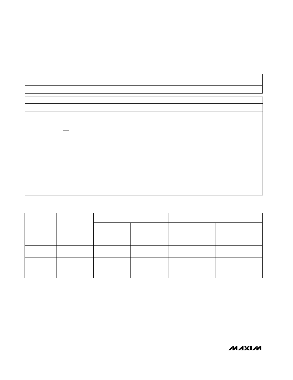
BIT
NAME
DESCRIPTION
7(MSB)
START
The first logic “1” bit after CS goes low defines the beginning of the control byte.
6
SEL2
These 3 bits select which of the eight channels are used for the conversion (Tables 1 and 2).
5 SEL1
4
SEL0
3
UNI/BIP
1 = unipolar, 0 = bipolar. Selects unipolar or bipolar conversion mode. In unipolar mode, an
analog input signal from 0 to V
REF
can be converted; in bipolar mode, the differential signal can
range from -V
REF
/2 to +V
REF
/2.
2
SGL/DIF
1 = single ended, 0 = pseudo-differential. Selects single-ended or pseudo-differential conver-
sions. In single-ended mode, input signal voltages are referred to COM. In pseudo-differential
mode, the voltage difference between two channels is measured (Tables 1 and 2).
1
PD1
Select operating mode.
0(LSB)
PD0
PD1
PD0
Mode
0
0
Full power-down
0
1
Fast power-down
1
0
Reduced power
1 1 Normal
operation
Table 3. Control-Byte Format
BIT 7
BIT 6
BIT 5
BIT 4
BIT 3
BIT 2
BIT 1
BIT 0
(MSB)
(LSB)
START
SEL2
SEL1
SEL0
UNI/BIP
SGL/DIF
PD1
PD0
Once conversion is completed, the device goes into
the programmed power mode until a new control byte
is written.
The power-up delay is dependent on the power-down
state. Software low-power modes will be able to start
conversion immediately when running at decreased
clock rates (see Power-Down Sequencing). Upon
power-on reset, when exiting software full power-down
mode, or when exiting hardware shutdown, the device
goes immediately into full-power mode and is ready to
convert after 2µs when using an external reference.
When using the internal reference, wait for the typical
power-up delay from a full power-down (software or
hardware) as shown in Figure 8.
PD1/PD0
MODE
TOTAL SUPPLY CURRENT
CIRCUIT SECTIONS*
CONVERTING
(mA)
AFTER
CONVERSION
INPUT COMPARATOR
REFERENCE
00
Full Power-Down
(FULLPD)
2.5
2µA
Off
Off
01
Fast Power-Down
(FASTPD)
2.5
0.9mA
Reduced Power
On
10
Reduced Power
Mode (REDP)
2.5
1.3mA
Reduced Power
On
11
Normal Operating
2.5
2.0 mA
Full Power
On
Table 4. Software-Controlled Power Modes
* Circuit operation between conversions; during conversion all circuits are fully powered up.