Internal and external references, Transfer function – Rainbow Electronics MAX1083 User Manual
Page 16
MAX1082/MAX1083
mode (PD1 = PD0 = 0), with an external reference and
conversion controlled at the maximum clock speed.
One dummy conversion to power up the device is
needed, but no waiting time is necessary to start the
second conversion, thereby achieving lower power
consumption at up to half the full sampling rate.
Using Fast Power-Down and Reduced
Power Modes
FASTPD and REDP modes achieve the lowest power
consumption at speeds close to the maximum sam-
pling rate. Figure 10 shows the MAX1083’s power con-
sumption in FASTPD mode (PD1 = 0, PD0 = 1), REDP
mode (PD1 = 1, PD0 = 0), and, for comparison, normal
operating mode (PD1 = 1, PD0 = 1). The figure shows
power consumption using the specified power-down
mode, with the internal reference and conversion con-
trolled at the maximum clock speed. The clock speed
in FASTPD or REDP should be limited to 4.8MHz for the
MAX1082/MAX1083. FULLPD mode may provide
increased power savings in applications where the
MAX1082/MAX1083 are inactive for long periods of
time, but intermittent bursts of high-speed conversions
are required.
Internal and External References
The MAX1082/MAX1083 can be used with an internal
or external reference voltage. An external reference
can be connected directly at REF or at the REFADJ pin.
An internal buffer is designed to provide 2.5V at
REF for the MAX1082/MAX1083. The internally trimmed
1.22V reference is buffered with a 2.05 gain.
Internal Reference
The MAX1082/MAX1083’s full-scale range with the
internal reference is 2.5V with unipolar inputs and
±1.25V with bipolar inputs. The internal reference volt-
age is adjustable by ±100mV with the circuit in Figure
12.
External Reference
The MAX1082/MAX1083’s external reference can be
placed at the input (REFADJ) or the output (REF) of the
internal reference-buffer amplifier. The REFADJ input
impedance is typically 17k
Ω. At REF, the DC input
resistance is a minimum of 18k
Ω. During conversion, an
external reference at REF must deliver up to 350µA DC
load current and have 10
Ω or less output impedance. If
the reference has a higher output impedance or is
noisy, bypass it close to the REF pin with a 4.7µF
capacitor.
To use the direct REF input, disable the internal buffer
by connecting REFADJ to V
DD1
. Using the REFADJ
input makes buffering the external reference unneces-
sary.
Transfer Function
Table 5 shows the full-scale voltage ranges for unipolar
and bipolar modes.
Figure 13 depicts the nominal, unipolar input/output
(I/O) transfer function, and Figure 14 shows the bipolar
I/O transfer function. Code transitions occur halfway
between successive-integer LSB values. Output coding
is binary, with 1LSB = 2.44mV (2.500V/2/1024) for
300ksps/400ksps, Single-Supply, 4-Channel,
Serial 10-Bit ADCs with Internal Reference
16
______________________________________________________________________________________
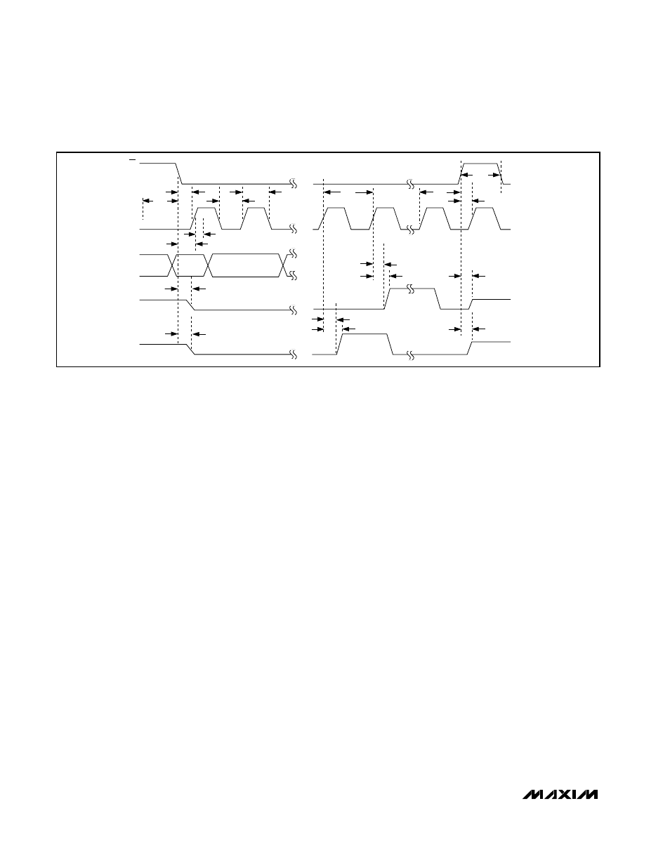
t
CSW
t
CP
t
CSH
t
CS1
t
STD
t
DOD
t
DOV
t
DOH
t
STV
t
STH
#10
SCLK
DIN
DOUT
SSTRB
t
CSS
t
CH
t
CSO
t
CL
t
DH
t
DOE
t
DS
t
STE
CS
Figure 6. Detailed Serial-Interface Timing