Max1802 digital camera step-down power supply – Rainbow Electronics MAX1802 User Manual
Page 8
MAX1802
Digital Camera Step-Down
Power Supply
8
_______________________________________________________________________________________
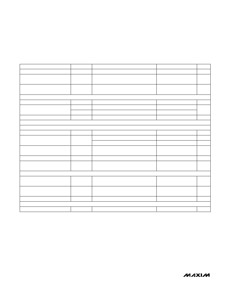
PARAMETER
SYMBOL
CONDITIONS
MIN
TYP
MAX
UNITS
FBC Input Leakage Current
V
FBC
= 1.35V
100
nA
COMPC Minimum Output
Voltage
V
FBC
= 1.35V, COMPC open
0.3
V
COMPC Maximum Output
Voltage
V
COMPC(MAX)
V
FBC
= 1.15V, COMPC open
2.00
2.27
V
CORE POWER SWITCHES (V
ONC
= 3V)
LXC Leakage Current
V
LXC
= 0, 5.5V
20
µA
R
DSN
N-channel, I
LXC
= 0.75A
350
Switch On-Resistance
R
DSP
P-channel, I
LXC
= 0.75A
400
m
Ω
N-Channel Turn-Off Current
5
190
mA
AUXILIARY DC-DC CONTROLLERS 1, 2, 3 (V
ON1
= V
DCON
_= 3V)
INTERNAL CLOCK
OSC Clock Low Trip Level
OSC falling edge
0.2
0.3
V
V
DCON
_ = 0.625V
0.575
0.675
V
OSC Clock High Trip Level
V
DCON
_ = 1.25V to V
VL
1.00
1.10
Maximum Duty Cycle
Adjustment Range
40
90
%
DCON_ Input Leakage Current
V
DCON
_ = 0V to 3V
1
µA
DCON_ Input Sleep-Mode
Threshold
V
DCON
_ rising, 50mV hysteresis
0.35
0.45
V
AUXILIARY ERROR AMPLIFIER
FB_ Regulation Voltage
Unity gain configuration, FB_ = COMP_
1.230
1.265
V
FB_ to COMP_
Transconductance
G
EA
Unity gain configuration, FB_ = COMP_,
-5µA < I
LOAD
< 5µA
70
160
µs
FB_ Input Leakage Current
V
FB
_ = 1.35V
100
nA
AUXILIARY DRIVERS (DL1, DL2, DL3)
DL_ Driver Resistance
Output high or low
11
Ω
ELECTRICAL CHARACTERISTICS (continued)
(Circuit of Figure 1, V
VDDM
= 6V, V
VDDC
= 3V, PGNDM = PGND = GND, DCON1 = REF, V
ONM
= 3V, V
ONC
= V
ON1
= V
DCON2
=
V
DCON3
= 0, T
A
= -40°C to +85°C, unless otherwise noted.) (Note 1)
Note 1: Specifications to -40
°C are guaranteed by design and not production tested.