Max1802 digital camera step-down power supply – Rainbow Electronics MAX1802 User Manual
Page 19
MAX1802
Digital Camera Step-Down
Power Supply
______________________________________________________________________________________
19
R
OSC
= (200ns - 1/f
OSC
) / (C
OSC
+ 10pF)
✕
ln (1 - V
REF
/ V
VL
)
See the Typical Operating Characteristics for f
OSC
vs.
R
OSC
using different values of C
OSC
. Due to duty cycle
limitation in the main controller, keep f
OSC
≤ V
MAIN
/
(V
VDDM(MAX)
✕
500ns).
Setting the Output Voltages
Set the MAX1802 output voltage of each converter by
connecting a resistive voltage-divider from the output
voltage to the corresponding FB_ input. The FB_ input
bias current is <100nA, so choose R
L
(the low-side
FB_-to-GND resistor) to be 100k
Ω. Choose R
H
(the
high-side output-to-FB_ resistor) according to the rela-
tion:
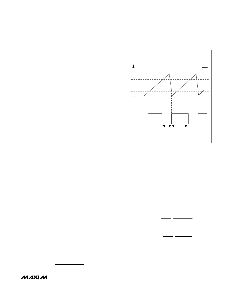
Setting the Maximum Duty Cycle
The oscillator signal at OSC and the voltage at DCON_
are used to generate the internal clock signals for the
three MAX1802 auxiliary controllers (CLK in Figure 3).
The internal clock’s falling edge occurs when V
OSC
exceeds V
DCON
_ (set by a resistive divider). The inter-
nal clock’s rising edge occurs when V
OSC
falls below
0.25V (Figure 5).
The adjustable maximum duty cycle range is 40% to
90% (see Maximum Duty Cycle vs. V
DCON
_ in the
Typical Operating Characteristics). The maximum duty
cycle defaults to 76% at 100kHz if V
DCON
_ is at or
above the voltage at V
REF
(1.25V) (see Default
Maximum Duty Cycle vs. Frequency in the Typical
Operating Characteristics). The controller shuts down if
V
DCON
_ is <0.3V.
Inductor Selection
Main and Core Step-Down Converters
MAX1802 main and core step-down converters offer
best efficiency when the inductor current is continuous.
For most designs, a reasonable inductor value (L
IDEAL
)
can be derived from the following equation, which sets
continuous peak-to-peak inductor current at 1/3 the DC
inductor current:
where D, the duty cycle, is given by:
In these equations, V
DSP
is the voltage drop across the
P-channel MOSFET switch, and V
DSN
is the voltage
drop across the N-channel MOSFET synchronous recti-
fier. Given L
IDEAL
, the consistent peak-to-peak inductor
current is 0.33 I
OUT
. The maximum inductor current is
1.17 I
OUT
.
Inductance values smaller than L
IDEAL
can be used;
however, the maximum inductor current will rise as L is
reduced, and a larger output capacitance will be
required to maintain the same output ripple. For stable
operation, the minimum inductance is limited by the
internal slope compensation. The minimum inductor
values for main and core are given by:
and
where R
DSP
is the on-resistance of the P-channel MOS-
FET switch, and D
MAX
= V
OUT
/ V
IN
.
Auxiliary Step-Up Controllers
The three MAX1802 auxiliary step-up controllers offer
best efficiency when the inductor current is continuous.
L
D
V
f
MIN CORE
MAX
OUT
OSC
(
)
.
.
=
−
1
0 5
0 13
L
D
V
R
f
MIN MAIN
MAX
OUT
DSP
OSC
(
)
.
.
=
−
1
0 5
0 013
D
V
V
V
V
V
OUT
DSN
IN
DSP
DSN
=
+
−
+
L
V
V
D
D
I
f
IDEAL
IN
DSP
OUT OSC
=
−
(
)
−
( )
3
1
R
R
V
H
L
OUT
=
−
1 248
1
.
t
L
t
H
1.25
V
OSC
(V)
V
DCON_
0.25
0
CLK
t
H
t
L
+ t
H
D
MAX
=
Figure 5. Auxiliary Controller Internal Clock Signal Generation