Max1802 digital camera step-down power supply – Rainbow Electronics MAX1802 User Manual
Page 7
MAX1802
Digital Camera Step-Down
Power Supply
_______________________________________________________________________________________
7
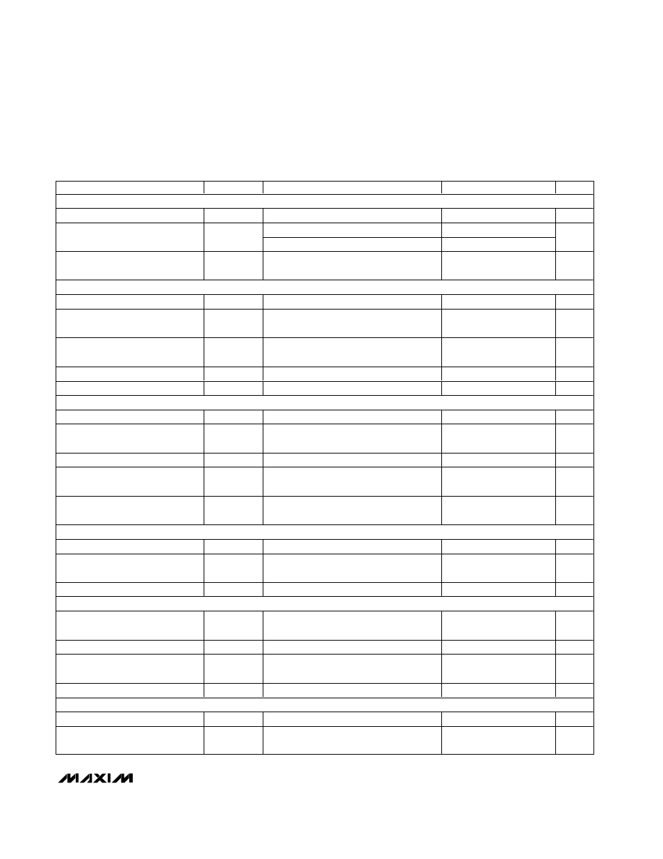
ELECTRICAL CHARACTERISTICS (continued)
(Circuit of Figure 1, V
VDDM
= 6V, V
VDDC
= 3V, PGNDM = PGND = GND, DCON1 = REF, V
ONM
= 3V, V
ONC
= V
ON1
= V
DCON2
=
V
DCON3
= 0, T
A
= -40°C to +85°C, unless otherwise noted.) (Note 1)
PARAMETER
SYMBOL
CONDITIONS
MIN
TYP
MAX
UNITS
LOGIC INPUTS (ONM, ONC, ON1)
Input Low Level
V
IL
0.4
V
ONM
1.8
Input High Level
V
IH
ONC, ON1
1.6
V
Input Leakage Current
ONM: V
IN
= 0 or 11V;
ONC, ON1: V
IN
= 0 or 5V
1
µA
MAIN DC-DC CONVERTER
Main Output Voltage Adjust Range
V
OUT
2.7
5.5
V
Main Idle Mode Threshold
V
OSC
= 0.625V, measured between
VDDM and LXM
2
35
mV
Main Current-Sense Amplifier
Voltage Gain
A
VCSM
Measured between VDDM and LXM
8.4
10.2
V/V
Main Zero-Crossing Threshold
Measured between LXM and PGNDM
-20
-8
mV
Main Slope Compensation Gain
A
VSWM
0.16
0.24
V/V
MAIN ERROR AMPLIFIER
FBM Regulation Voltage
Unity gain configuration, FBM = COMPM
1.230
1.265
V
FBM to COMPM
Transconductance
G
EA
U ni ty g ai n confi g ur ati on, FBM = C OM P M ,
- 5
µA < I
LOA D
< 5
µA
70
160
µS
FBM Input Leakage Current
V
FBM
= 1.35V
100
nA
COMPM Minimum Output
Voltage
V
FBM
= 1.35V, COMPM open
0.3
V
COMPM Maximum Output
Voltage
V
COMPM(MAX)
V
FBM
= 1.15V, COMPM open
2.00
2.27
V
MAIN DRIVERS (DHM, DLM)
Output Low Voltage
I
SINK
= 10mA
0.11
V
Output High Voltage
I
SOURCE
= 10mA
V
VDDM
-
0.11
V
Driver Resistance
I
DHM
= 10mA, I
DLM
= 10mA
11
Ω
CORE DC-DC CONVERTER (V
ONC
= 3V)
Core Output Voltage Adjust
Range
V
OUT
1.25
5.5
V
Core Idle Mode Threshold
V
OSC
= 0.625V
40
360
mA
Core Current-Sense Amplifier
Transresistance
R
CSC
0.7
1.3
V/A
Core Slope Compensation Gain
A
VSWC
0.16
0.24
V/V
CORE ERROR AMPLIFIER (V
ONC
= 3V)
FBC Regulation Voltage
Unity gain configuration, FBC = COMPC
1.230
1.265
V
FBC to COMPC
Transconductance
G
EA
U ni ty g ai n confi g ur ati on, FBC = C OM P C ,
- 5
µA < I
LOA D
< 5
µA
70
160
µS