Max1802 digital camera step-down power supply, Pin description – Rainbow Electronics MAX1802 User Manual
Page 12
MAX1802
Digital Camera Step-Down
Power Supply
12
______________________________________________________________________________________
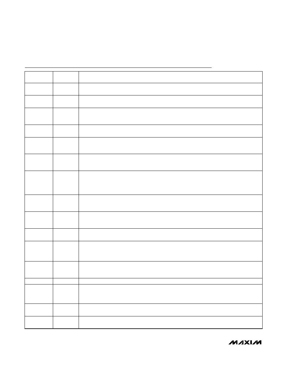
Pin Description
PIN
NAME
FUNCTION
1
FBM
Main DC-DC Converter Feedback Input. Connect a feedback resistive voltage-divider from the output
to FBM to set the main output voltage. Regulation voltage is V
REF
(1.25V).
2
COMPM
Compensation for Main Controller. Output of main transconductance error amplifier. Connect a series
resistor and capacitor to GND to compensate the main control loop (see Compensation Design).
3
ONM
Main Converter Enable Input. High level turns on the main converter and VL regulator. Connect ONM
to VDDM to automatically start the converter. When the main converter is off, all other outputs are
disabled.
4
VH
Internal Bias Voltage. VH provides bias to the main controller. Bypass VH to VDDM with a 0.1µF or
greater ceramic capacitor.
5
VDDM
Battery Input. VDDM supplies power to the IC and also serves as a high-side current-sense input
for the main DC-DC controller. Connect VDDM as close as possible to the source of the external
P-channel switching MOSFET for the main controller.
6
DHM
External P-Channel MOSFET Gate-Drive Output for Main Controller. DHM swings between VDDM and
PGNDM with 400mA (typ) drive current. Connect DHM to the gate of the external P-channel switching
MOSFET for the main controller.
7
LXM
Main DC-DC Controller Current-Sense Input. Connect LXM to the drains of the external P- and N-
channel switching MOSFETs for the main converter. LXM serves as the current-sense input for both
P- and N-channel switching MOSFETs. Connect LXM as close as possible to the drain of the external
P-channel switching MOSFET for the main controller.
8
DLM
External N-Channel MOSFET Gate-Drive Output for Main Controller. DLM swings between VDDM
and PGNDM with 400mA (typ) drive current. Connect DLM to the gate of the external N-channel
switching MOSFET for the main controller.
9
PGNDM
P ow er G r ound for M ai n D C - D C C ontr ol l er . P G N D M al so ser ves as a l ow - si d e cur r ent- sense i np ut for
the m ai n D C - D C contr ol l er . C onnect P GN D M as cl ose as p ossi b l e to the sour ce of the exter nal
N - channel sw i tchi ng M OS FE T for the m ai n contr ol l er .
10
OSC
Oscillator Control. Connect a timing capacitor from OSC to GND and a timing resistor from OSC to VL
to set the switching frequency between 100kHz and 1MHz (see Setting the Switching Frequency).
11
DCON1
Maximum Duty Cycle Control Input for Auxiliary Controller 1. Connect DCON1 to VL to set the default
maximum duty cycle. Connect a resistive voltage-divider from REF to DCON1 to set the maximum
duty cycle between 40% and 90%. Pull DCON1 below 300mV to turn the controller off.
12
DL1
External MOSFET Gate Drive Output for Auxiliary Controller 1. DL1 swings between VDDC and PGND
with 400mA (typ) drive current. Connect DL1 to the gate of the external switching N-channel MOSFET
for auxiliary controller 1.
13
ON1
Enable Input for Auxiliary Controller 1. Connect ON1 to VL to automatically start auxiliary controller 1.
14
COMP1
Compensation for Auxiliary Controller 1. Output of auxiliary controller 1 transconductance error
amplifier. Connect a series resistor and capacitor from COMP1 to GND to compensate the auxiliary
controller 1 control loop (see Compensation Design).
15
FB1
Feedback Input for Auxiliary Controller 1. Connect a feedback resistive voltage-divider from the
output of auxiliary controller 1 to FB1 to set the output voltage. Regulation voltage is V
REF
(1.25V).
16
FB2
Feedback Input for Auxiliary Controller 2. Connect a feedback resistive voltage-divider from the
output of auxiliary controller 2 to FB2 to set the output voltage. Regulation voltage is V
REF
(1.25V).