Detailed description, Pseudo-differential input – Rainbow Electronics MAX1204 User Manual
Page 8
MAX1204
5V, 8-Channel, Serial, 10-Bit ADC
with 3V Digital Interface
8
_______________________________________________________________________________________
_______________Detailed Description
The MAX1204 uses a successive-approximation con-
version technique and input track/hold (T/H) circuitry to
convert an analog signal to a 10-bit digital output. A
flexible serial interface provides easy interface to 3V
microprocessors (µPs). Figure 3 is the MAX1204 block
diagram.
Pseudo-Differential Input
Figure 4 shows the analog-to-digital converter’s
(ADC’s) analog comparator’s sampling architecture. In
single-ended mode, IN+ is internally switched to
CH0–CH7 and IN- is switched to GND. In differential
mode, IN+ and IN- are selected from pairs of CH0/CH1,
CH2/CH3, CH4/CH5, and CH6/CH7. Configure the
channels using Tables 3 and 4.
In differential mode, IN- and IN+ are internally switched
to either of the analog inputs. This configuration is
pseudo-differential such that only the signal at IN+ is
sampled. The return side (IN-) must remain stable with-
in ±0.5LSB (±0.1LSB for best results) with respect to
GND during a conversion. To do this, connect a 0.1µF
capacitor from IN- (of the selected analog input) to
GND.
During the acquisition interval, the channel selected as
the positive input (IN+) charges capacitor C
HOLD
. The
acquisition interval spans three SCLK cycles and ends
on the falling SCLK edge after the input control word’s
last bit is entered. The T/H switch opens at the end of
the acquisition interval, retaining charge on C
HOLD
as a
sample of the signal at IN+.
The conversion interval begins with the input multiplex-
er switching C
HOLD
from the positive input (IN+) to the
negative input (IN-). In single-ended mode, IN- is sim-
ply GND. This unbalances node ZERO at the compara-
tor’s input. The capacitive DAC adjusts during the
remainder of the conversion cycle to restore node
ZERO to 0V within the limits of 10-bit resolution. This
action is equivalent to transferring a charge of 16pF x
[(V
IN
+) - (V
IN
-)] from C
HOLD
to the binary-weighted
capacitive DAC, which in turn forms a digital represen-
tation of the analog input signal.
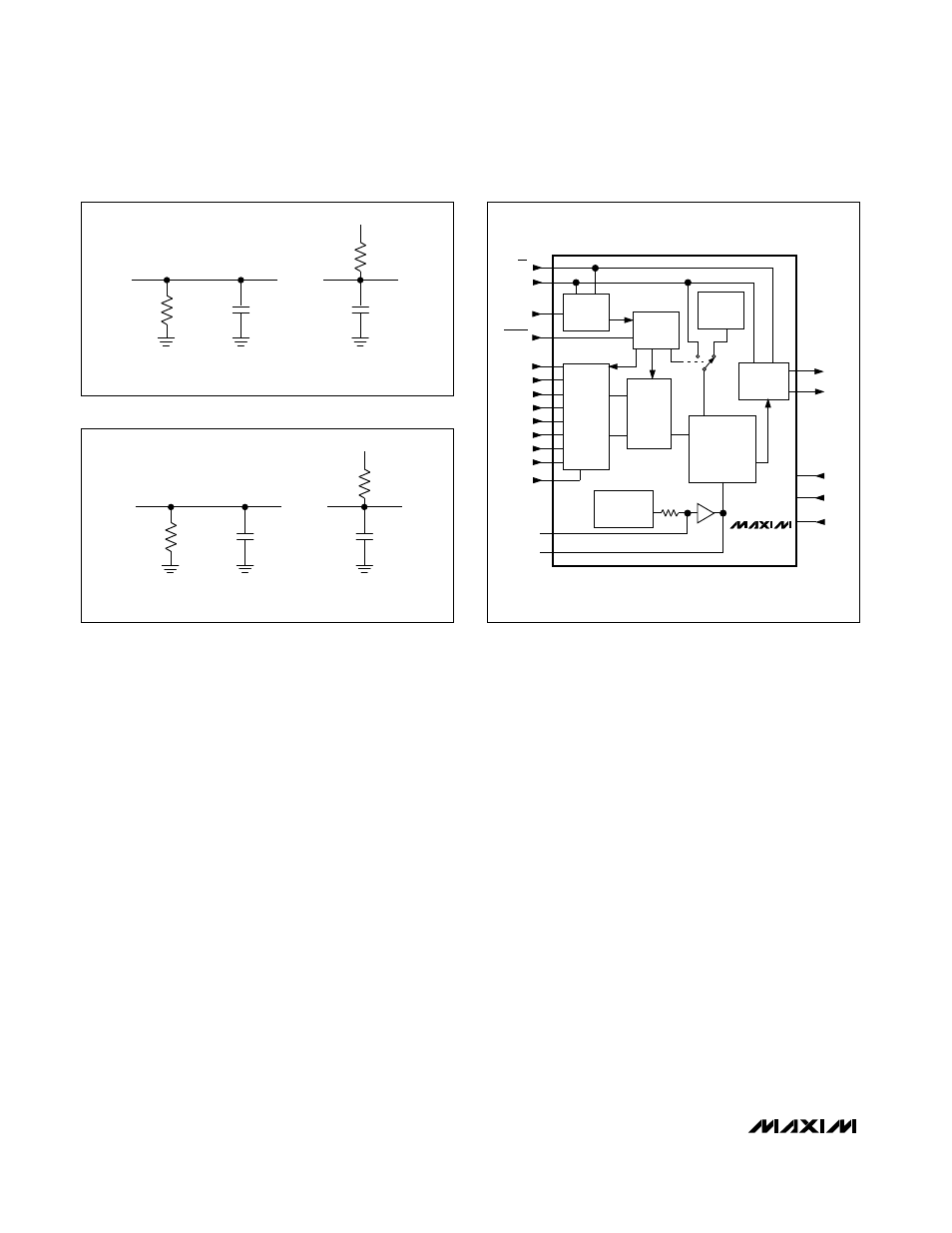
Figure 1. Load Circuits for Enable Time
Figure 2. Load Circuits for Disable Time
Figure 3. Block Diagram
+3.3V
3k
C
LOAD
GND
DOUT
C
LOAD
GND
3k
DOUT
a. High-Z to V
OH
and V
OL
to V
OH
b. High-Z to V
OL
and V
OH
to V
OL
+3.3V
3k
C
LOAD
GND
DOUT
C
LOAD
GND
3k
DOUT
a. V
OH
to High-Z
b. V
OL
to High-Z
INPUT
SHIFT
REGISTER
CONTROL
LOGIC
INT
CLOCK
OUTPUT
SHIFT
REGISTER
+2.44V
REFERENCE
T/H
ANALOG
INPUT
MUX
SAR
ADC
IN
DOUT
SSTRB
V
DD
VL
V
SS
SCLK
DIN
CH0
CH1
CH3
CH2
CH7
CH6
CH5
CH4
GND
REFADJ
REF
OUT
REF
CLOCK
+4.096V
20k
≈
1.68
1
2
3
4
5
6
7
8
10
11
12
13
15
16
17
18
19
MAX1204
CS
SHDN
A
20
14
9