Typical operating characteristics, Pin description – Rainbow Electronics MAX1204 User Manual
Page 7
MAX1204
5V, 8-Channel, Serial, 10-Bit ADC
with 3V Digital Interface
_______________________________________________________________________________________
7
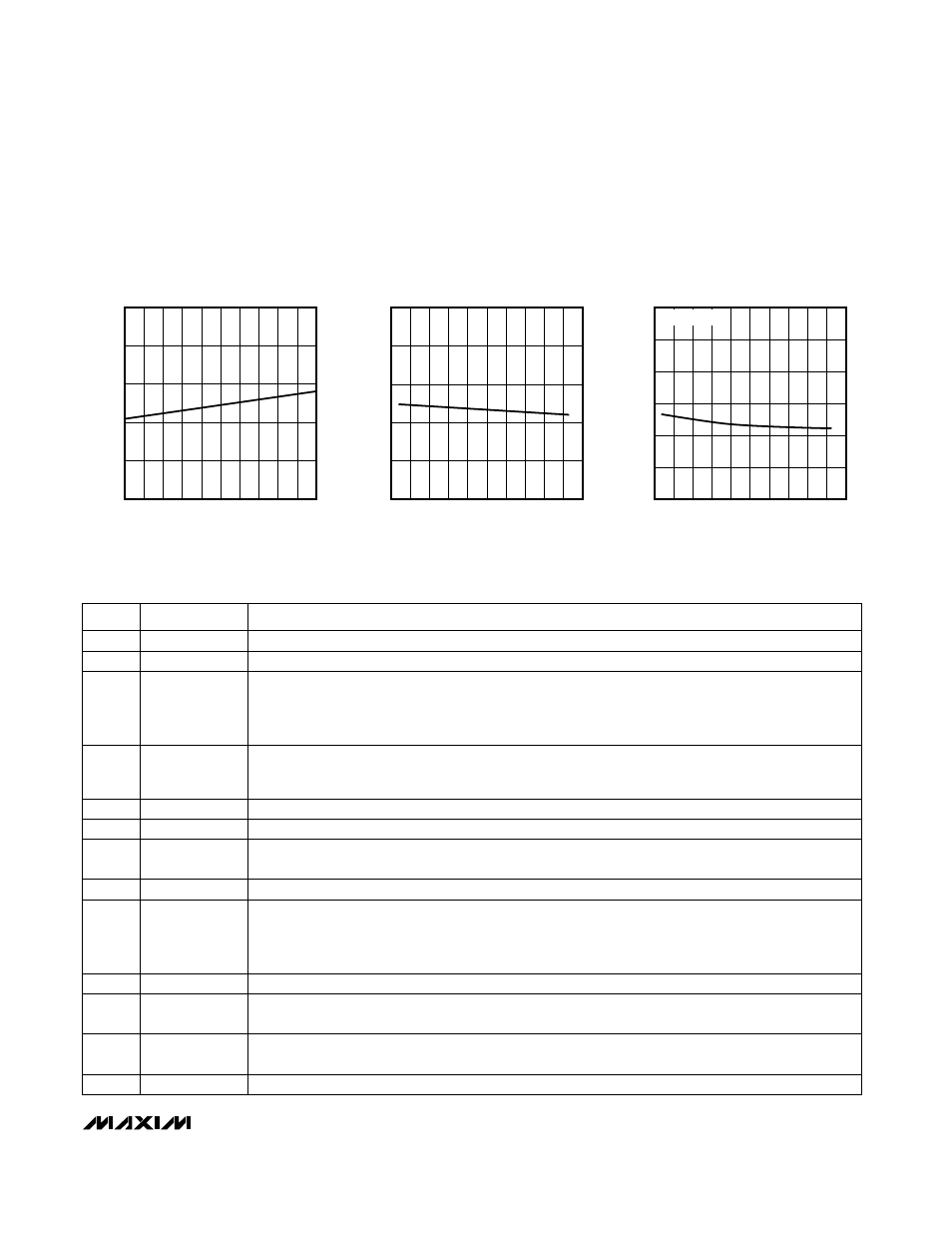
1.0
2.0
1.8
1.6
1.4
1.2
4.5
SUPPLY CURRENT
vs. SUPPLY VOLTAGE
MAX1204 TOC01
SUPPLY VOLTAGE (V)
SUPPLY CURRENT (mA)
5.3
4.7
5.1
5.5
4.9
1.0
-60
SUPPLY CURRENT
vs. TEMPERATURE
1.2
MAX1204 TOC02
TEMPERATURE (°C)
SUPPLY CURRENT (mA)
100
1.6
1.4
-20
60
140
2.0
1.8
20
6
5
0
-60
SHUTDOWN SUPPLY CURRENT
vs. TEMPERATURE
4
MAX1204 TOC03
TEMPERATURE (
°
C)
SHUTDOWN SUPPLY CURRENT (
µ
A)
60
2
1
-20
20
3
100
140
REFADJ = GND
__________________________________________Typical Operating Characteristics
(V
DD
= 5V ±5%; VL = 2.7V to 3.6V; f
SCLK
= 2.0MHz, external clock (50% duty cycle); 15 clocks/conversion cycle (133ksps);
4.7µF capacitor at REF; T
A
= +25°C; unless otherwise noted.)
NAME
FUNCTION
1–8
CH0–CH7
Sampling Analog Inputs
9
V
SS
Negative Supply Voltage. Tie V
SS
to -5V ±5% or GND.
PIN
10
SHDN
Three-Level Shutdown Input. Pulling
SHDN low shuts the MAX1204 down to 10µA (max) supply
current; otherwise, the MAX1204 is fully operational. Pulling
SHDN to V
DD
puts the reference-buffer
amplifier in internal compensation mode. Letting
SHDN float puts the reference-buffer amplifier in
external compensation mode.
11
REF
Reference Buffer Output/ADC Reference Input. In internal reference mode, the reference buffer
provides a 4.096V nominal output, externally adjustable at REFADJ. In external reference mode,
disable the internal buffer by pulling REFADJ to V
DD.
15
DOUT
Serial-Data Output. Data is clocked out at SCLK’s falling edge. High impedance when
CS is high.
14
VL
Supply Voltage for Digital Output Pins. Voltage applied to VL determines the positive output swing of
the Digital Outputs (DOUT, SSTRB).
13
GND
Ground; IN- Input for Single-Ended Conversions
12
REFADJ
Input to the Reference-Buffer Amplifier. Tie REFADJ to V
DD
to disable the reference-buffer amplifier.
20
V
DD
Positive Supply Voltage, +5V ±5%
19
SCLK
Serial-Clock Input. SCLK clocks data in and out of serial interface. In external clock mode, SCLK also
sets the conversion speed. (Duty cycle must be 40% to 60% in external clock mode.)
18
CS
Active-Low Chip Select. Data is not clocked into DIN unless
CS is low. When CS is high, DOUT is
high impedance.
17
DIN
Serial-Data Input. Data is clocked in at SCLK’s rising edge.
16
SSTRB
Serial-Strobe Output. In internal clock mode, SSTRB goes low when the MAX1204 begins the analog-
to-digital conversion and goes high when the conversion is finished. In external clock mode, SSTRB
pulses high for one clock period before the MSB decision. High impedance when
CS is high (external
clock mode).
______________________________________________________________Pin Description