Applications information, Power-on reset, Reference-buffer compensation – Rainbow Electronics MAX1204 User Manual
Page 15: Power-down
MAX1204
5V, 8-Channel, Serial, 10-Bit ADC
with 3V Digital Interface
______________________________________________________________________________________
15
__________ Applications Information
Power-On Reset
When power is first applied and if
SHDN is not pulled
low, internal power-on reset circuitry activates the
MAX1204 in internal clock mode, ready to convert with
SSTRB = high. After the power supplies are stabilized,
the internal reset time is 100µs. No conversions should
be performed during this phase. SSTRB is high on
power-up, and if
CS is low, the first logical 1 on DIN is
interpreted as a start bit. Until a conversion takes
place, DOUT shifts out zeros.
Reference-Buffer Compensation
In addition to its shutdown function,
SHDN also selects
internal or external compensation. The compensation
affects both power-up time and maximum conversion
speed. Compensated or not, the minimum clock rate is
100kHz due to droop on the sample-and-hold.
Float
SHDN to select external compensation. The
Typical
Operating Circuit
uses a 4.7µF capacitor at REF. A value
of 4.7µF or greater ensures stability and allows converter
operation at the 2MHz full clock speed. External com-
pensation increases power-up time (see the section
Choosing Power-Down Mode,
and Table 5).
Internal compensation requires no external capacitor at
REF, and is selected by pulling
SHDN high. Internal com-
pensation allows for the shortest power-up times, but is
only available using an external clock up to 400kHz.
Power-Down
Choosing Power-Down Mode
You can save power by placing the converter in a
low-current shutdown state between conversions.
Select full power-down or fast power-down mode via
bits 1 and 0 of the DIN control byte with
SHDN high or
floating (Tables 2 and 6). Pull
SHDN low at any time to
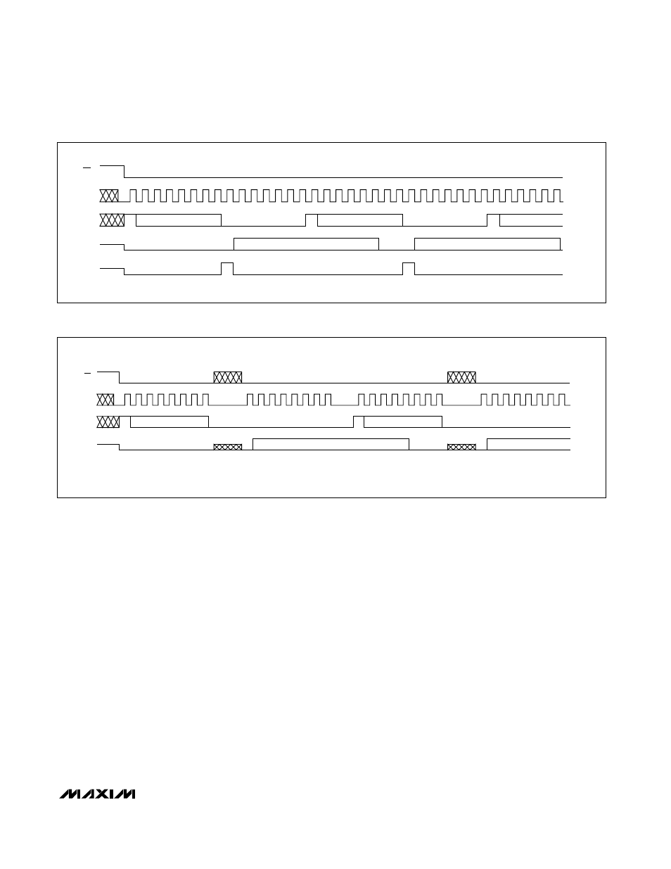
Figure 11a. External Clock Mode, 15 Clocks/Conversion Timing
Figure 11b. External Clock Mode, 16 Clocks/Conversion Timing
SCLK
DIN
DOUT
CS
S
CONTROL BYTE 0
CONTROL BYTE 1
S
CONVERSION RESULT 0
CONVERSION RESULT 1
SSTRB
CONTROL BYTE 2
S
1
8
1
8
1
15
15
B2
B3
B4
B5
B6
B7
B8
B9
B1 B0 S1 S0
B2
B3
B4
B5
B6
B7
B8
B9
B1 B0 S1 S0
CS
SCLK
DIN
DOUT
S
CONTROL BYTE 0
CONTROL BYTE 1
S
CONVERSION RESULT 0
CONVERSION RESULT 1
• • •
• • •
• • •
• • •
B2
B3
B4
B5
B6
B7
B8
B9
B5
B6
B7
B8
B9
B1 B0 S1 S0