Table 5. typical power-up delay times – Rainbow Electronics MAX1204 User Manual
Page 16
MAX1204
5V, 8-Channel, Serial, 10-Bit ADC
with 3V Digital Interface
16
______________________________________________________________________________________
shut down the converter completely.
SHDN overrides
bits 1 and 0 of the control byte.
Full power-down mode turns off all chip functions
that draw quiescent current, reducing I
DD
and I
SS
typi-
cally to 2µA.
Fast power-down mode turns off all circuitry except the
bandgap reference. With fast power-down mode, the
supply current is 30µA. Power-up time can be shortened
to 5µs in internal compensation mode.
The I
DD
shutdown current can increase if any digital input
(DIN, SCLK,
CS) is held high in either power-down mode.
The actual shutdown current depends on the state of the
digital inputs, the voltage applied to the digital inputs
(V
IH
), the supply voltage (V
DD
), and the operating temper-
ature. Figure 12c shows the maximum I
DD
increase for
each digital input held high in power-down mode for differ-
ent operating conditions. This current is cumulative, so if
all three digital inputs are held high, the additional shut-
down current is three times the value shown in Figure 12c.
In both software power-down modes, the serial interface
remains operational, but the ADC does not convert.
Table 5 shows how the choice of reference-buffer com-
pensation and power-down mode affects both power-up
delay and maximum sample rate.
In external compensation mode, power-up time is 20ms
with a 4.7µF compensation capacitor (200ms with a 33µF
capacitor) when the capacitor is initially fully discharged.
From fast power-down, start-up time can be eliminated
by using low-leakage capacitors that do not discharge
more than 1/2LSB while shut down. In power-down, the
capacitor has to supply the current into the reference
(typically 1.5µA) and the transient currents at power-up.
Figures 12a and 12b show the various power-down
sequences in both external and internal clock modes.
Software Power-Down
Software power-down is activated using bits PD1 and
PD0 of the control byte. As shown in Table 6, PD1 and
PD0 also specify clock mode. When software power-
down is asserted, the ADC continues to operate in the
last specified clock mode until the conversion is com-
plete. The ADC then powers down into a low
quiescent-current state. In internal clock mode, the
interface remains active and conversion results can be
clocked out even though the MAX1204 has already
entered a software power-down.
The first logical 1 on DIN is interpreted as a start bit
and powers up the MAX1204. Following the start bit,
the control byte also determines clock and power-down
modes. For example, if the control byte contains PD1 =
1, the chip remains powered up. If PD1 = 0,
power-down resumes after one conversion.
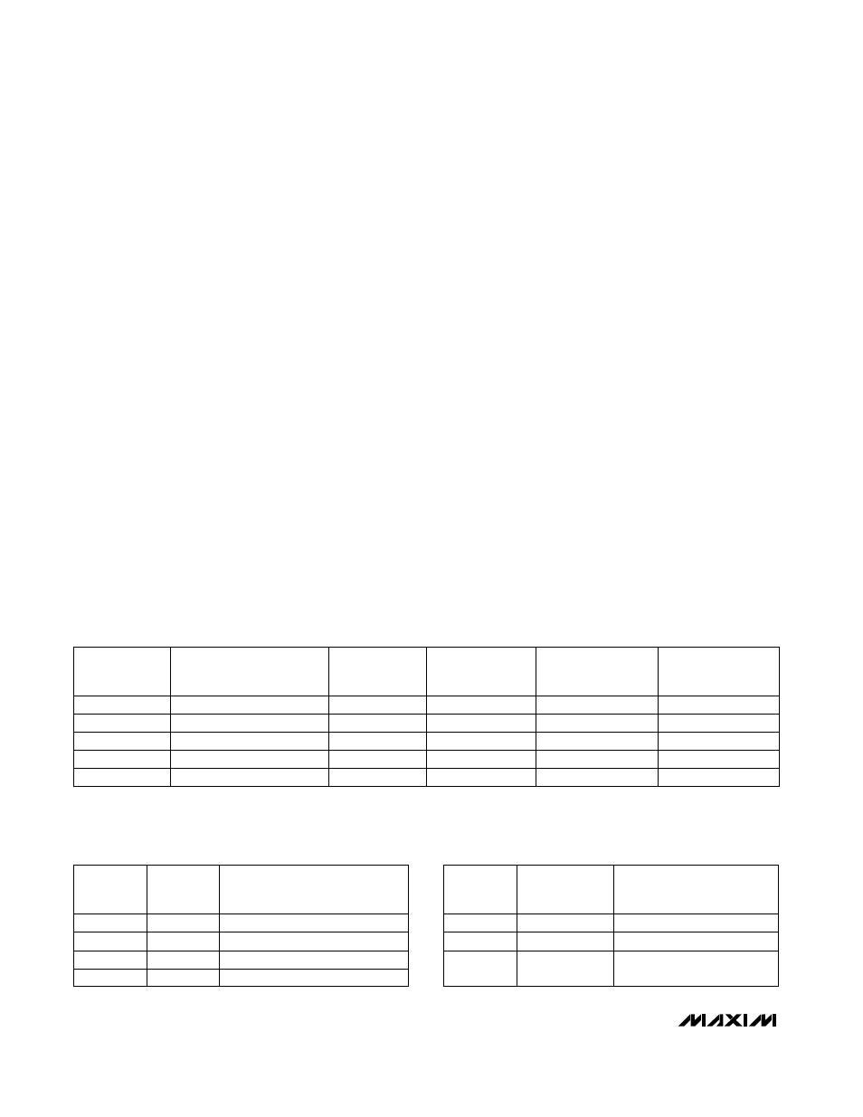
Table 5. Typical Power-Up Delay Times
133
2
Full
Disabled
133
2
Fast
Disabled
133
26
26
MAXIMUM
SAMPLING RATE
(ksps)
See Figure 14c
300
5
POWER-UP
DELAY (µs)
Fast/Full
Full
Fast
POWER-DOWN
MODE
4.7
REFERENCE
CAPACITOR
(µF)
External
Enabled
REFERENCE
BUFFER
Internal
Enabled
Internal
Enabled
REFERENCE-BUFFER
COMPENSATION MODE
Full power-down mode
0
0
Fast power-down mode
1
0
PD1
Internal clock mode
0
1
External clock mode
1
1
DEVICE MODE
PD0
N/A
Full
Power-Down
GND
SHDN
STATE
External compensation
Enabled
Floating
Internal compensation
Enabled
V
DD
REFERENCE-BUFFER
COMPENSATION
DEVICE
MODE
Table 6. Software Shutdown and
Clock Mode
Table 7. Hard-Wired Shutdown and
Compensation Mode