Rainbow Electronics MAX1204 User Manual
Page 21
MAX1204
5V, 8-Channel, Serial, 10-Bit ADC
with 3V Digital Interface
______________________________________________________________________________________
21
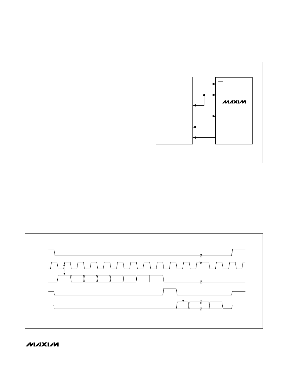
TMS320CL3x to MAX1204 Interface
Figure 19 shows an application circuit to interface the
MAX1204 to the TMS320 in external clock mode. Figure
20 is the timing diagram for this interface circuit.
Use the following steps to initiate a conversion in the
MAX1204 and to read the results.
1) The TMS320 should be configured with CLKX (trans-
mit clock) as an active-high output clock and CLKR
(TMS320 receive clock) as an active-high input clock.
The TMS320’s CLKX and CLKR are tied together with
the MAX1204’s SCLK input.
2) The MAX1204’s
CS is driven low by the TMS320’s
XF_ I/O port to enable data to be clocked into the
MAX1204’s DIN.
3) Write an 8-bit word (1XXXXX11) to the MAX1204 to
initiate a conversion and place the device into exter-
nal clock mode. Refer to Table 2 to select the proper
XXXXX bit values for your specific application.
4) The MAX1204’s SSTRB output is monitored via the
TMS320’s FSR input. A falling edge on the SSTRB
output indicates that the conversion is in progress
and data is ready to be received from the MAX1204.
5) The TMS320 reads in one data bit on each of the
next 16 rising edges of SCLK. These data bits repre-
sent the 10-bit conversion result followed by two
sub-bits and four trailing bits, which should be
ignored.
6) Pull
CS high to disable the MAX1204 until the next
conversion is initiated.
Figure 19. MAX1204 to TMS320 Serial Interface
XF
CLKX
CLKR
DX
DR
FSR
CS
SCLK
DIN
DOUT
SSTRB
TMS320LC3x
MAX1204
Figure 20. TMS320 Serial-Interface Timing Diagram
CS
SCLK
DIN
SSTRB
DOUT
START
SEL2
SEL1
SEL0
UNI/BIP SGL/DIF
PD1
PD0
MSB
LSB
HIGH
IMPEDANCE
HIGH
IMPEDANCE