Data framing – Rainbow Electronics MAX1204 User Manual
Page 14
MAX1204
5V, 8-Channel, Serial, 10-Bit ADC
with 3V Digital Interface
14
______________________________________________________________________________________
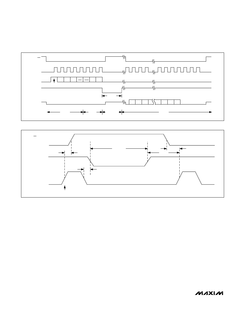
Figure 9. Internal Clock Mode Timing
SSTRB
CS
SCLK
DIN
DOUT
1
4
8
12
18
20
24
START
SEL2 SEL1 SEL0
UNI/
DIP
SGL/
DIF
PD1 PD0
B9
MSB
B8
B7
B0
LSB
S1
S0
ACQUISITION
1.5µs
(SCLK = 2MHz)
IDLE
FILLED WITH
ZEROS
IDLE
CONVERSION
10µs MAX
ADC STATE
2
3
5
6
7
9
10
11
19
21
22
23
t
CONV
Data Framing
CS’s falling edge does
not
start a conversion on the
MAX1204. The first logic high clocked into DIN is inter-
preted as a start bit and defines the first bit of the control
byte. A conversion starts on SCLK’s falling edge after the
eighth bit of the control byte (the PD0 bit) is clocked into
DIN. The start bit is defined as:
The first high bit clocked into DIN with
CS low any-
time the converter is idle; (e.g., after V
DD
is applied).
or
The first high bit clocked into DIN after bit 3 (B3) of a
conversion in progress appears at DOUT.
If a falling edge on
CS forces a start bit before B3
becomes available, the current conversion is termi-
nated and a new one started. Thus, the fastest the
MAX1204 can run is 15 clocks/conversion. Figure 11a
shows the serial-interface timing necessary to perform
a conversion every 15 SCLK cycles in external clock
mode. If
CS is low and SCLK is continuous, guarantee
a start bit by first clocking in 16 zeros.
Most microcontrollers (µCs) require that conversions
occur in multiples of eight SCLK clocks; 16 clocks per
conversion is typically the fastest that a µC can drive
the MAX1204. Figure 11b shows the serial-interface
timing necessary to perform a conversion every 16
SCLK cycles in external clock mode.
Figure 10. Internal Clock Mode SSTRB Detailed Timing
PD0 CLOCK IN
t
SSTRB
t
CSH
t
CONV
t
SCK
SSTRB
• • •
SCLK
• • •
t
CSS
NOTE: KEEP SCLK LOW DURING CONVERSION FOR BEST NOISE PERFORMANCE.
CS
• • •