External and internal references, Transfer function and gain adjust – Rainbow Electronics MAX1204 User Manual
Page 18
MAX1204
5V, 8-Channel, Serial, 10-Bit ADC
with 3V Digital Interface
18
______________________________________________________________________________________
Lowest Power at Higher Throughputs
Figure 14b shows power consumption with external-
reference compensation in fast power-down, with one and
eight channels converted. The external 4.7µF compensa-
tion requires a 50µs wait after power-up. This circuit com-
bines fast multichannel conversion with the lowest power
consumption possible. Full power-down mode can
increase power savings in applications where the
MAX1204 is inactive for long periods of time, but where
intermittent bursts of high-speed conversions are required.
External and Internal References
The MAX1204 can be used with an internal or external
reference. An external reference can be connected
directly at the REF terminal or at the REFADJ pin.
An internal buffer is designed to provide 4.096V at REF
for the MAX1204. Its internally trimmed 2.44V reference
is buffered with a 1.68 nominal gain.
Internal Reference
The MAX1204’s full-scale range with internal reference is
4.096V with unipolar inputs and ±2.048V with bipolar
inputs. The internal reference voltage is adjustable to
±1.5% with the circuit of Figure 17.
External Reference
An external reference can be placed at either the input
(REFADJ) or the output (REF) of the MAX1204’s internal
buffer amplifier. The REFADJ input impedance is typical-
ly 20k
Ω
. At REF, the input impedance is a minimum of
12k
Ω
for DC currents. During conversion, an external
reference at REF must deliver up to 350µA DC load cur-
rent and have an output impedance of 10
Ω
or less. If the
reference has higher output impedance or is noisy,
bypass it close to the REF pin with a 4.7µF capacitor.
Using the buffered REFADJ input makes buffering of
the external reference unnecessary. To use the direct
REF input, disable the internal buffer by tying REFADJ
to V
DD
. In power-down, the input bias current to
REFADJ can be as much as 25µA with REFADJ tied to
V
DD
. Pull REFADJ to GND to minimize the input bias
current in power-down.
Transfer Function and Gain Adjust
Figure 15 depicts the nominal, unipolar input/output
(I/O) transfer function, and Figure 16 shows the bipolar
I/O transfer function. Code transitions occur halfway
between successive integer LSB values. Output coding
is binary with 1 LSB = 4mV (4.096V/1024) for
unipolar operation and 1 LSB = 4mV [(4.096V/2 -
-4.096V/2)/1024] for bipolar operation.
Figure 13. MAX1204 FULLPD/FASTPD Power-Up Sequence
1
0 0
DIN
REFADJ
REF
2.5V
0V
4V
0V
1
0 1
1
1
1
1
0 0
1
0 1
FULLPD
FASTPD
NOPD
FULLPD
FASTPD
2ms WAIT
COMPLETE CONVERSION SEQUENCE
t
BUFFEN
≈
15µs
τ
= RC = 20k
Ω
x C
REFADJ
(ZEROS)
CH1
CH7
(ZEROS)
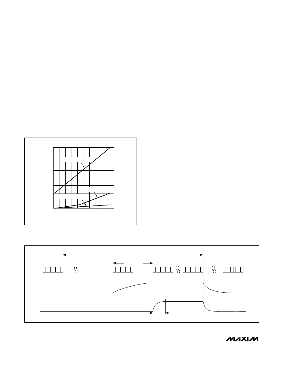
Figure 12c. Additional I
DD
Shutdown Supply Current vs. V
IH
for Each Digital Input at a Logic 1
0
-60
10
5
TEMPERATURE (°C)
SUPPLY CURRENT PER INPUT (
µ
A)
100
25
20
15
-20
60
140
40
35
30
20
(V
DD
- V
IH
) = 1.95V
(V
DD
- V
IH
) = 2.55V
(V
DD
- V
IH
) = 2.25V