Electrical characteristics (continued) – Rainbow Electronics MAX1314 User Manual
Page 6
MAX1304–MAX1306/MAX1308–MAX1310/MAX1312–MAX1314
8-/4-/2-Channel, 12-Bit, Simultaneous-Sampling ADCs
with ±10V, ±5V, and 0 to +5V Analog Input Ranges
6
_______________________________________________________________________________________
Note 1:
For the MAX1304/MAX1305/MAX1306, V
IN
= 0 to +5V. For the MAX1308/MAX1309/MAX1310, V
IN
= -5V to +5V. For the
MAX1312/MAX1313/MAX1314, V
IN
= -10V to +10V.
Note 2:
All channel performance is guaranteed by correlation to a single channel test.
Note 3:
The analog input resistance is terminated to an internal bias point (Figure 5). Calculate the analog input current using:
for V
CH
within the input voltage range.
Note 4:
Throughput rate is given per channel. Throughput rate is a function of clock frequency (f
CLK
). The external clock through-
put rate is specified with f
CLK
= 16.67MHz and the internal clock throughput rate is specified with f
CLK
= 15MHz. See the
Data Throughput section for more information.
Note 5:
The REF input resistance is terminated to an internal +2.5V bias point (Figure 2). Calculate the REF input current using:
for V
REF
within the input voltage range.
Note 6:
The REF
MS
input resistance is terminated to an internal +2.5V bias point (Figure 2). Calculate the REF
MS
input current using:
for V
REFMS
within the input voltage range.
Note 7:
All analog inputs are driven with a -0.4dBFS 500kHz sine wave.
Note 8:
Shutdown current is measured with the analog input floating. The large amplitude of the maximum shutdown current speci-
fication is due to automated test equipment limitations.
Note 9:
CONVST must remain low for at least the acquisition period. The maximum acquisition time is limited by internal capacitor droop.
Note 10:
CS to WR and CS to RD are internally AND together. Setup and hold times do not apply.
Note 11:
Minimum CLK frequency is limited only by the internal T/H droop rate. Limit the time between the rising edge of CONVST
and the falling edge of EOLC to a maximum of 1ms.
I
V
V
R
REFMS
REFMS
REFMS
=
− 2 5
.
I
V
V
R
REF
REF
REF
=
− 2 5
.
I
V
V
R
CH
CH
BIAS
CH
_
_
_
=
−
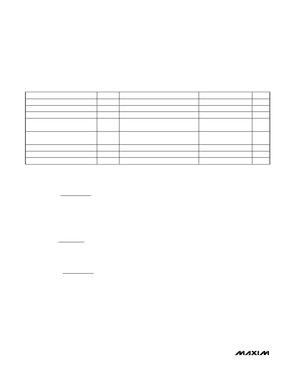
PARAMETER
SYMBOL
CONDITIONS
MIN
TYP
MAX
UNITS
Input-Data Setup Time
t
DTW
Figure 6
10
ns
Input-Data Hold Time
t
WTD
Figure 6
10
ns
External CLK Period
t
CLK
Figures 8, 9
0.05
10.00
µs
External CLK High Period
t
CLKH
Logic sensitive to rising edges,
Figures 8, 9
20
ns
External CLK Low Period
t
CLKL
Logic sensitive to rising edges,
Figures 8, 9
20
ns
External Clock Frequency
f
CLK
(Note 11)
0.1
20
MHz
Internal Clock Frequency
f
INT
15
MHz
CONVST High to CLK Edge
t
CNTC
Figures 8, 9
20
ns
ELECTRICAL CHARACTERISTICS (continued)
(AV
DD
= +5V, DV
DD
= +3V, AGND = DGND = 0, V
REF
= V
REFMS
= +2.5V (external reference), C
REF
= C
REFMS
= 0.1µF, C
REF+
=
C
REF-
= 0.1µF, C
REF+-to-REF-
= 2.2µF || 0.1µF, C
COM
= 2.2µF || 0.1µF, C
MSV
= 2.2µF || 0.1µF (unipolar devices), MSV = AGND (bipo-
lar devices), f
CLK
= 16.67MHz 50% duty cycle, INTCLK/EXTCLK = AGND (external clock), SHDN = DGND, T
A
= T
MIN
to T
MAX
,
unless otherwise noted. Typical values are at T
A
= +25°C. See Figures 3 and 4.)