Table 7. ±10v bipolar code table – Rainbow Electronics MAX1314 User Manual
Page 29
MAX1304–MAX1306/MAX1308–MAX1310/MAX1312–MAX1314
8-/4-/2-Channel, 12-Bit, Simultaneous-Sampling ADCs
with ±10V, ±5V, and 0 to +5V Analog Input Ranges
______________________________________________________________________________________
29
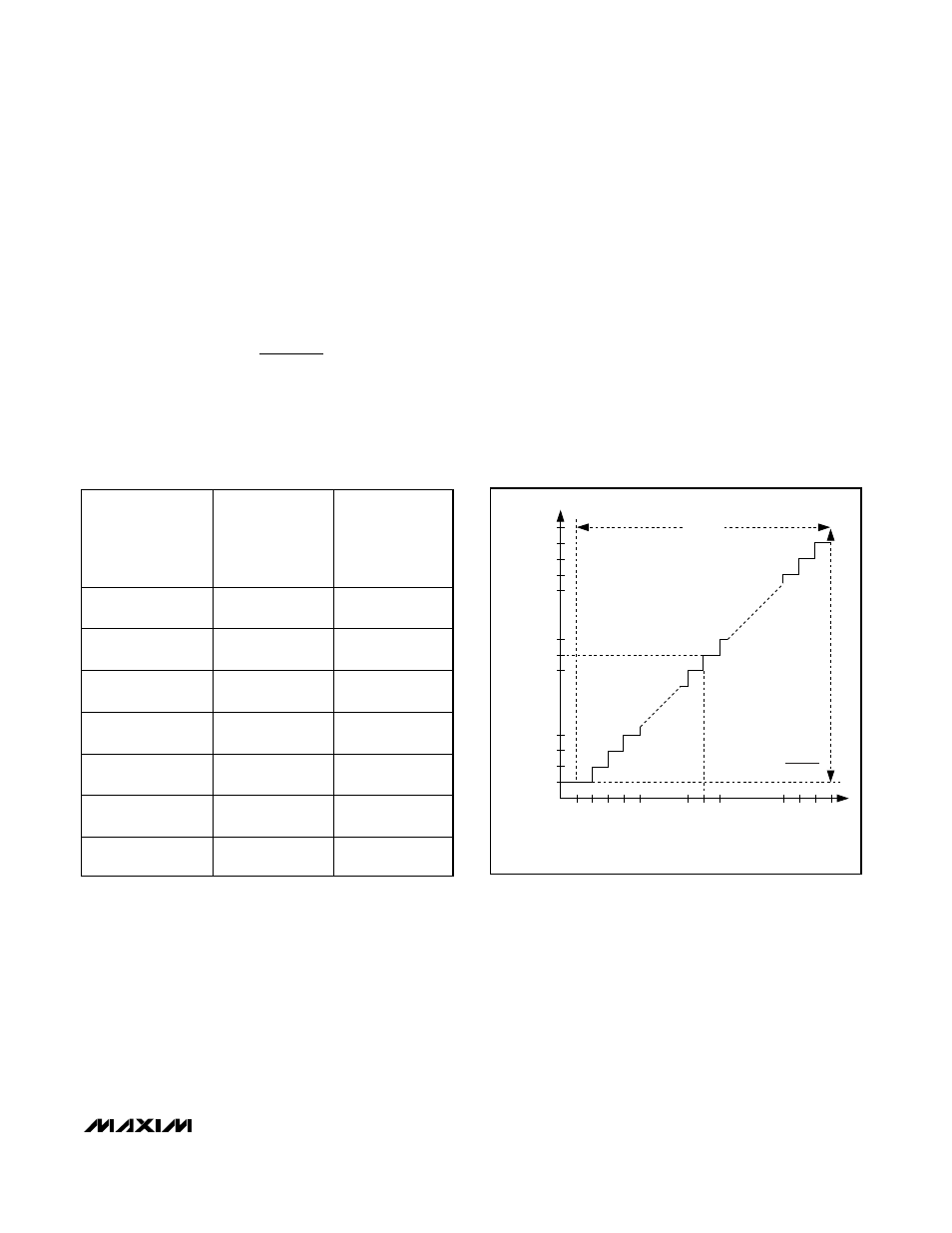
Bipolar ±10V Devices
Table 7 and Figure 14 show the two’s complement trans-
fer function for the ±10V input range MAX1312/
MAX1313/MAX1314. The FSR is eight times the voltage at
REF. The internal +2.5V reference gives a +20V FSR,
while an external +2V to +3V reference allows an FSR of
+16V to +24V, respectively. Calculate the LSB size using:
which equals 4.88mV with a +2.5V internal reference.
The input range is centered about V
MSV
. Normally,
MSV = AGND, and the input is symmetrical about zero.
For a custom midscale voltage, drive MSV with an
external voltage source. Noise present on MSV directly
couples into the ADC result. Use a precision, low-drift
voltage reference with adequate bypassing to prevent
MSV from degrading ADC performance. For maximum
FSR, do not violate the absolute maximum voltage rat-
ings of the analog inputs when choosing MSV.
Determine the input voltage as a function of V
REF
,
V
MSV
, and the output code in decimal using:
V
CH_
= LSB x CODE
10
+ V
MSV
1
8
2
12
LSB
x V
REF
=
Table 7. ±10V Bipolar Code Table
TWO’s
COMPLEMENT
DIGITAL OUTPUT
CODE
DECIMAL
EQUIVALENT
DIGITAL OUTPUT
CODE
(CODE
10
)
INPUT VOLTAGE
(V)
V
REF
= +2.5V
V
MSV
= 0
0111 1111 1111 =
0x7FF
+2047
+9.9976 ± 0.5 LSB
0111 1111 1110 =
0x7FE
+2046
+9.9927 ± 0.5 LSB
0000 0000 0001 =
0x001
+1
+0.0073 ± 0.5 LSB
0000 0000 0000 =
0x000
0
0.0024 ± 0.5 LSB
1111 1111 1111 =
0xFFF
-1
-0.0024 ± 0.5 LSB
1000 0000 0001 =
0x801
-2047
-9.9927 ± 0.5 LSB
1000 0000 0000 =
0x800
-2048
-9.9976 ± 0.5 LSB
(
)
8 x V
REF
8 x V
REF
2
12
1 LSB =
TWO'S COMPLEMENT BINAR
Y OUTPUT CODE
-2048 -2046
+2047
+2045
0x800
0x801
0x802
0x803
0x7FF
0x7FE
0x7FD
0x7FC
0xFFF
0x000
0x001
-1 0 +1
(MSV)
INPUT VOLTAGE (V
CH_
- V
MSV
IN LSBs)
Figure 14. ±10V Bipolar Transfer Function