Definitions – Rainbow Electronics MAX1314 User Manual
Page 32
MAX1304–MAX1306/MAX1308–MAX1310/MAX1312–MAX1314
8-/4-/2-Channel, 12-Bit, Simultaneous-Sampling ADCs
with ±10V, ±5V, and 0 to +5V Analog Input Ranges
32
______________________________________________________________________________________
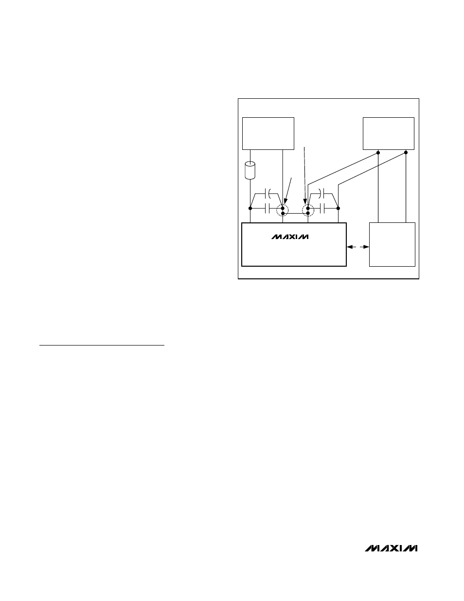
Layout, Grounding, and Bypassing
For best performance use PC boards. Board layout must
ensure that digital and analog signal lines are separated
from each other. Do not run analog and digital lines paral-
lel to one another (especially clock lines), and do not run
digital lines underneath the ADC package.
Figure 17 shows the recommended system ground con-
nections. Establish an analog ground point at AGND and
a digital ground point at DGND. Connect all analog
grounds to the analog ground point. Connect all digital
grounds to the digital ground point. For lowest noise
operation, make the power-supply ground returns as low
impedance and as short as possible. Connect the analog
ground point to the digital ground point at one location.
High-frequency noise in the power supplies degrades
the ADC’s performance. Bypass the analog power
plane to the analog ground plane with a 2.2µF capaci-
tor within one inch of the device. Bypass each AV
DD
to
AGND pair of pins with a 0.1µF capacitor as close to
the device as possible. AV
DD
to AGND pairs are pin 1
to pin 2, pin 14 to pin 15, and pin 16 to pin 17.
Likewise, bypass the digital power plane to the digital
ground plane with a 2.2µF capacitor within one inch of
the device. Bypass each DV
DD
to DGND pair of pins
with a 0.1µF capacitor as close to the device as possi-
ble. DV
DD
to DGND pairs are pin 24 to pin 25, and pin
38 to pin 39. If a supply is very noisy use a ferrite bead
as a lowpass filter as shown in Figure 17.
Definitions
Integral Nonlinearity (INL)
INL is the deviation of the values on an actual transfer
function from a straight line. For these devices, this
straight line is drawn between the endpoints of the
transfer function, once offset and gain errors have
been nullified.
Differential Nonlinearity (DNL)
DNL is the difference between an actual step width and
the ideal value of 1 LSB. For these devices, the DNL of
each digital output code is measured and the worst-
case value is reported in the electrical characteristics
table. A DNL error specification of less than ±1 LSB
guarantees no missing codes and a monotonic
transfer function.
Offset Error
Offset error is a figure of merit that indicates how well
the actual transfer function matches the ideal transfer
function at a single point. Typically the point at which
offset error is specified is either at or near the zero-
scale point of the transfer function or at or near the mid-
scale point of the transfer function.
For the unipolar devices (MAX1304/MAX1305/
MAX1306), the ideal zero-scale transition from 0x000 to
0x001 occurs at 1 LSB above AGND (Figure 12, Table 5).
Unipolar offset error is the amount of deviation between
the measured zero-scale transition point and the ideal
zero-scale transition point.
For the bipolar devices (MAX1308/MAX1309/MAX1310/
MAX1312/MAX1313/MAX1314), the ideal midscale tran-
sition from 0xFFF to 0x000 occurs at MSV (Figures 14
and 13, Tables 7 and 6). The bipolar offset error is the
amount of deviation between the measured midscale
transition point and the ideal midscale transition point.
ANALOG SUPPLY
AV
DD
AGND
DV
DD
DATA
DGND
DIGITAL
CIRCUITRY
OPTIONAL
FERRITE
BEAD
+5V
RETURN
DIGITAL
GROUND
POINT
DIGITAL SUPPLY
RETURN +3V TO +5V
DGND
DV
DD
MAX1304–MAX1306
MAX1308–MAX1310
MAX1312–MAX1314
ANALOG
GROUND
POINT
Figure 17. Power-Supply Grounding and Bypassing