Applications information, Table 2. configuration register – Rainbow Electronics MAX1314 User Manual
Page 21
MAX1304–MAX1306/MAX1308–MAX1310/MAX1312–MAX1314
8-/4-/2-Channel, 12-Bit, Simultaneous-Sampling ADCs
with ±10V, ±5V, and 0 to +5V Analog Input Ranges
______________________________________________________________________________________
21
Applications Information
Digital Interface
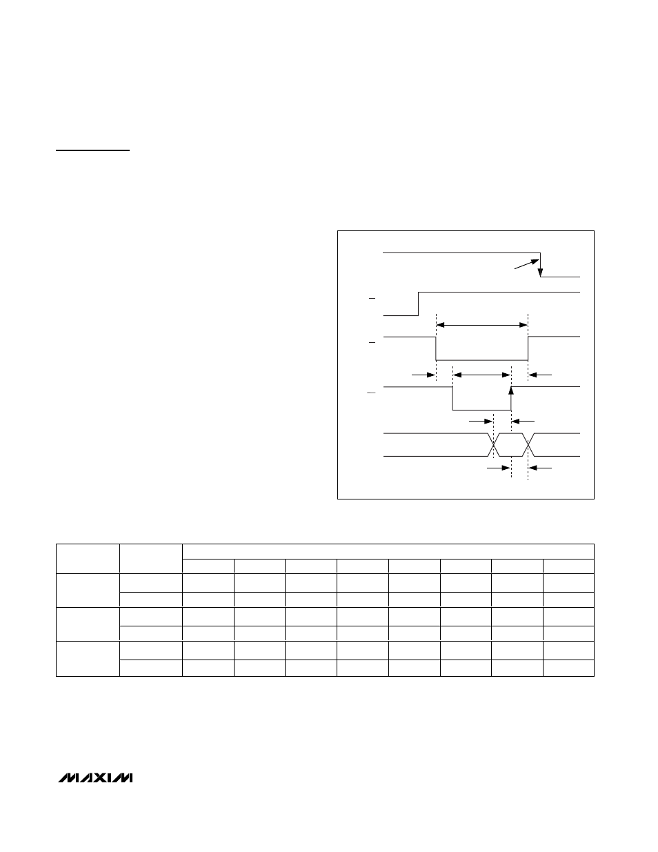
The bidirectional parallel digital interface allows for setting
the 8-bit configuration register (see the Configuration
Register section) and reading the 12-bit conversion
result. The interface includes the following control signals:
chip select (CS), read (RD), write (WR), end of conversion
(EOC), end of last conversion (EOLC), conversion start
(CONVST), shutdown (SHDN), channel shutdown
(CHSHDN), internal clock select (INTCLK/EXTCLK), and
external clock input (CLK). Figures 6, 7, 8, 9, Table 2, and
the Timing Characteristics show the operation of the inter-
face. D0–D7 are bidirectional, and D8–D11 are output
only. D0–D11 go high impedance when RD = 1 or CS = 1.
Configuration Register
Enable channels as active by writing to the configura-
tion register through I/O lines D0–D7 (Table 2). The bits
in the configuration register map directly to the chan-
nels, with D0 controlling channel zero, and D7 control-
ling channel seven. Setting any bit high activates the
corresponding input channel, while resetting any bit
low deactivates the corresponding channel. On the
devices with less than eight channels, some of the bits
have no function (Table 2).
To write to the configuration register, pull CS and WR
low, load bits D0 through D7 onto the parallel bus, and
force WR high. The data are latched on the rising edge
of WR (Figure 6). Write to the configuration register at
any point during the conversion sequence. At power-
up, write to the configuration register to select the
active channels before beginning a conversion.
However, the new configuration does not take effect
until the next CONVST falling edge. At power-up all
channels default active. Shutdown does not change the
configuration register. The configuration register may
be written to in shutdown. See the Channel Shutdown
(CHSHDN) section for information about using the con-
figuration register for power saving.
Table 2. Configuration Register
BIT/CHANNEL
PART
NUMBER
STATE
D0/CH0
D1/CH1
D2/CH2
D3/CH3
D4/CH4
D5/CH5
D6/CH6
D7/CH7
ON
1
1
1
1
1
1
1
1
MAX1304
MAX1308
MAX1312
OFF
0
0
0
0
0
0
0
0
ON
1
1
1
1
X
X
X
X
MAX1305
MAX1309
MAX1313
OFF
0
0
0
0
X
X
X
X
ON
1
1
X
X
X
X
X
X
MAX1306
MAX1310
MAX1314
OFF
0
0
X
X
X
X
X
X
X = Don’t care (must be 1 or 0).
D0–D7
DATA-IN
RD
CONVST
CONFIGURATION
REGISTER UPDATES
CS
WR
t
CS
t
WRL
t
CTW
t
DTW
t
WTD
t
WTC
Figure 6. Write Timing