Table 3. reference bypass capacitors, Table 4. reference voltages – Rainbow Electronics MAX1314 User Manual
Page 26
MAX1304–MAX1306/MAX1308–MAX1310/MAX1312–MAX1314
8-/4-/2-Channel, 12-Bit, Simultaneous-Sampling ADCs
with ±10V, ±5V, and 0 to +5V Analog Input Ranges
26
______________________________________________________________________________________
To avoid the timing requirements associated with pow-
ering up an analog channel, force CHSHDN high. With
CHSHDN high, each analog input is powered up
regardless of whether it is selected for conversion in
the configuration register. Note that shutdown mode
takes precedence over the CHSHDN mode.
Reference
Internal Reference
The internal reference circuits provide for analog input
voltages of 0 to +5V for the unipolar MAX1304/
MAX1305/MAX1306, ±5V for the bipolar MAX1308/
MAX1309/MAX1310 or ±10V for the bipolar MAX1312/
MAX1313/MAX1314. Install external capacitors for ref-
erence stability, as indicated in Table 3 and shown in
Figures 3 and 4.
As illustrated in Figure 2, the internal reference voltage
is 2.5V (V
REF
). This 2.5V is internally buffered to create
the voltages at REF+ and REF-. Table 4 shows the volt-
ages at COM, REF+, and REF-.
External Reference
External reference operation is achieved by overriding
the internal reference voltage. Override the internal ref-
erence voltage by driving REF with a +2.0V to +3.0V
external reference. As shown in Figure 2, the REF input
impedance is 5kΩ. For more information about using
external references see the Transfer Functions section.
Midscale Voltage (MSV)
The voltage at MSV (V
MSV
) sets the midpoint of the ADC
transfer functions. For the 0 to +5V input range (unipolar
devices), the midpoint of the transfer function is +2.5V.
For the ±5V and ±10V input range devices, the midpoint
of the transfer function is zero.
As shown in Figure 2, there is a unity-gain buffer
between REF
MS
and MSV in the unipolar MAX1304/
MAX1305/MAX1306. This midscale buffer sets the mid-
point of the unipolar transfer functions to either the inter-
nal +2.5V reference or an externally applied voltage at
REF
MS
. V
MSV
follows V
REFMS
within ±3mV.
The midscale buffer is not active for the bipolar
devices. For these devices, MSV must be connected to
AGND or externally driven. REF
MS
must be bypassed
with a 0.01µF capacitor to AGND.
See the Transfer Functions section for more information
about MSV.
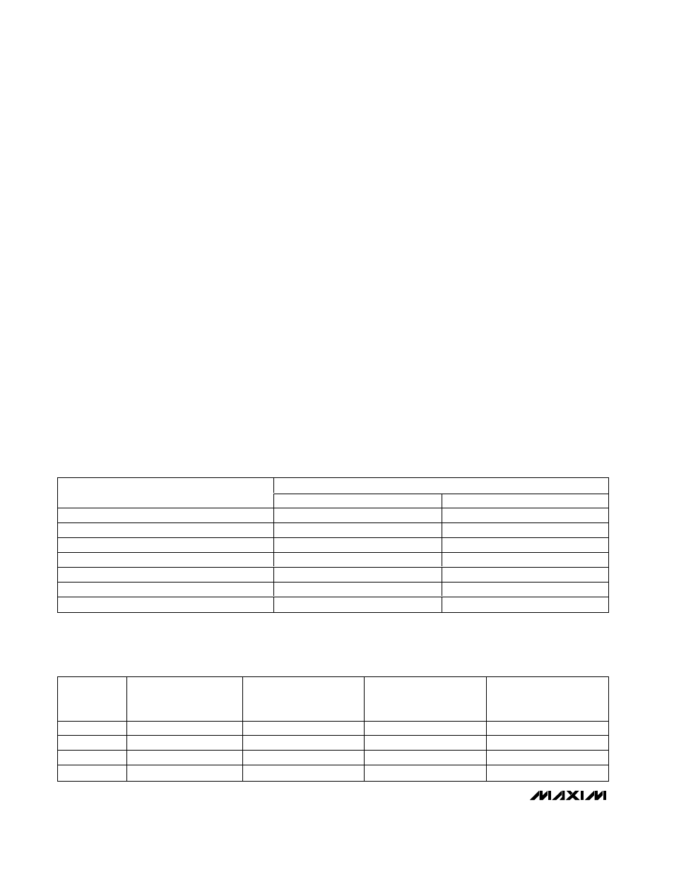
Table 3. Reference Bypass Capacitors
INPUT VOLTAGE RANGE
LOCATION
UNIPOLAR (µF)
BIPOLAR (µF)
MSV Bypass Capacitor to AGND
2.2 || 0.1
N/A
REF
MS
Bypass Capacitor to AGND
0.01
0.01
REF Bypass Capacitor to AGND
0.01
0.01
REF+ Bypass Capacitor to AGND
0.1
0.1
REF+ to REF- Capacitor
2.2 || 0.1
2.2 || 0.1
REF- Bypass Capacitor to AGND
0.1
0.1
COM Bypass Capacitor to AGND
2.2 || 0.1
2.2 || 0.1
Table 4. Reference Voltages
PARAMETER
EQUATION
CALCULATED VALUE (V)
V
REF
= 2.000V,
AV
DD
= 5.0V
CALCULATED VALUE (V)
V
REF
= 2.500V,
AV
DD
= 5.0V
CALCULATED VALUE (V)
V
REF
= 3.000V,
AV
DD
= 5.0V
V
COM
V
COM
= 13 / 25 x AV
DD
2.600
2.600
2.600
V
REF+
V
REF+
= V
COM
+ V
REF
/ 2
3.600
3.850
4.100
V
REF-
V
REF-
= V
COM
- V
REF
/ 2
1.600
1.350
1.100
V
REF+
- V
REF-
V
REF-
- V
REF+
= V
REF
2.000
2.500
3.000
(
)
(
)
(
)
N/A = Not applicable. Connect MSV directly to AGND.