Pin description – Rainbow Electronics MAX1314 User Manual
Page 13
MAX1304–MAX1306/MAX1308–MAX1310/MAX1312–MAX1314
8-/4-/2-Channel, 12-Bit, Simultaneous-Sampling ADCs
with ±10V, ±5V, and 0 to +5V Analog Input Ranges
______________________________________________________________________________________
13
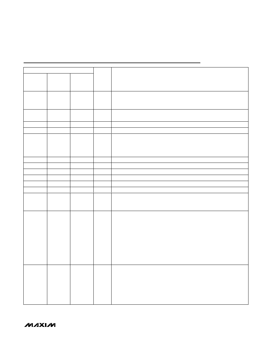
Pin Description
PIN
MAX1304
MAX1308
MAX1312
MAX1305
MAX1309
MAX1313
MAX1306
MAX1310
MAX1314
NAME
FUNCTION
1, 15, 17
1, 15, 17
1, 15, 17
AV
DD
Analog Power Input. AV
DD
is the power input for the analog section of the
converter. Apply +5V to AV
DD
.
Connect all AV
DD
pins together.
See the Layout,
Grounding, and Bypassing section for additional information.
2, 3, 14,
16, 23
2, 3, 14,
16, 23
2, 3, 14,
16, 23
AGND
Analog Ground. AGND is the power return for AV
DD
.
Connect all AGND
pins together.
4
4
4
CH0
Channel 0 Analog Input
5
5
5
CH1
Channel 1 Analog Input
6
6
6
MSV
Midscale Voltage Bypass.
For the unipolar MAX1304/MAX1305/MAX1306,
connect a 2.2µF and a 0.1µF capacitor from MSV to AGND. For the bipolar
MAX1308/MAX1309/MAX1310/MAX1312/MAX1313/MAX1314, connect
MSV to AGND.
7
7
—
CH2
Channel 2 Analog Input
8
8
—
CH3
Channel 3 Analog Input
9
—
—
CH4
Channel 4 Analog Input
10
—
—
CH5
Channel 5 Analog Input
11
—
—
CH6
Channel 6 Analog Input
12
—
—
CH7
Channel 7 Analog Input
13
13
13
INTCLK/
EXTCLK
Clock-Mode Select Input.
Connect INTCLK/EXTCLK to AV
DD
to select the
internal clock. Connect INTCLK/EXTCLK to AGND to use an external clock
connected to CLK.
18
18
18
REF
MS
Midscale Reference Bypass or Input.
REF
MS
connects through a 5k
Ω
resistor to
the internal +2.5V bandgap reference buffer.
For the MAX1304/MAX1305/MAX1306 unipolar devices, V
REFMS
is the input to
the unity-gain buffer that drives MSV.
MSV sets the midpoint of the input voltage
range.
For internal reference operation, bypass REF
MS
with a
≥
0.01µF
capacitor to AGND.
For external reference operation, drive REF
MS
with an
external voltage from +2V to +3V.
For the MAX1308/MAX1309/MAX1310/MAX1312/MAX1313/MAX1314 bipolar
devices, connect REF
MS
to REF.
For internal reference operation, bypass the
REF
MS
/REF node with a
≥
0.01µF capacitor to AGND.
For external reference
operation, drive the REF
MS
/REF node with an external voltage from +2V to +3V.
19
19
19
REF
ADC Reference Bypass or Input. REF connects through a 5k
Ω
resistor to the
internal +2.5V bandgap reference buffer.
For internal reference operation, bypass REF with a
≥
0.01µF capacitor.
For external reference operation with the MAX1304/MAX1305/MAX1306
unipolar devices, drive REF with an external voltage from +2V to +3V.
For external reference operation with the MAX1308/MAX1309/MAX1310/
MAX1312/MAX1313/MAX1314 bipolar devices, connect REF
MS
to REF and
drive the REF
MS
/REF node with an external voltage from +2V to +3V.