Pin description (continued) – Rainbow Electronics MAX1314 User Manual
Page 14
MAX1304–MAX1306/MAX1308–MAX1310/MAX1312–MAX1314
8-/4-/2-Channel, 12-Bit, Simultaneous-Sampling ADCs
with ±10V, ±5V, and 0 to +5V Analog Input Ranges
14
______________________________________________________________________________________
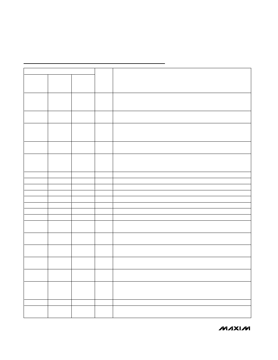
Pin Description (continued)
PIN
MAX1304
MAX1308
MAX1312
MAX1305
MAX1309
MAX1313
MAX1306
MAX1310
MAX1314
NAME
FUNCTION
20
20
20
REF+
Positive Reference Bypass.
Bypass REF+ with a 0.1µF capacitor to AGND. Also
bypass REF+ to REF- with a 2.2µF and a 0.1µF capacitor.
V
REF+
= V
COM
+ V
REF
/ 2.
21
21
21
COM
Reference Common Bypass.
Bypass COM to AGND with a 2.2µF and a 0.1µF
capacitor.
V
COM
= 13 / 25 x AV
DD
.
22
22
22
REF-
Negative Reference Bypass.
Bypass REF- with a 0.1µF capacitor to AGND.
Also bypass REF- to REF+ with a 2.2µF and a 0.1µF capacitor.
V
REF+
= V
COM
- V
REF
/ 2.
24, 39
24, 39
24, 39
DGND
Digital Ground. DGND is the power return for DV
DD
.
Connect all DGND
pins together.
25, 38
25, 38
25, 38
DV
DD
Digital Power Input. DV
DD
powers the digital section of the converter, including
the parallel interface. Apply +2.7V to +5.25V to DV
DD
. Bypass DV
DD
to DGND
with a 0.1µF capacitor.
Connect all DV
DD
pins together.
26
26
26
D0
D i g i tal I/O 0 of 12- Bi t P ar al l el D ata Bus.
H i g h i m p ed ance w hen RD = 1 or CS = 1.
27
27
27
D1
D i g i tal I/O 1 of 12- Bi t P ar al l el D ata Bus.
H i g h i m p ed ance w hen RD = 1 or CS = 1.
28
28
28
D2
D i g i tal I/O 2 of 12- Bi t P ar al l el D ata Bus.
H i g h i m p ed ance w hen RD = 1 or CS = 1.
29
29
29
D3
D i g i tal I/O 3 of 12- Bi t P ar al l el D ata Bus.
H i g h i m p ed ance w hen RD = 1 or CS = 1.
30
30
30
D4
D i g i tal I/O 4 of 12- Bi t P ar al l el D ata Bus.
H i g h i m p ed ance w hen RD = 1 or CS = 1.
31
31
31
D5
D i g i tal I/O 5 of 12- Bi t P ar al l el D ata Bus.
H i g h i m p ed ance w hen RD = 1 or CS = 1.
32
32
32
D6
D i g i tal I/O 6 of 12- Bi t P ar al l el D ata Bus.
H i g h i m p ed ance w hen RD = 1 or CS = 1.
33
33
33
D7
D i g i tal I/O 7 of 12- Bi t P ar al l el D ata Bus.
H i g h i m p ed ance w hen RD = 1 or CS = 1.
34
34
34
D8
Digital Output 8 of 12-Bit Parallel Data Bus.
High impedance when RD = 1 or
CS = 1.
35
35
35
D9
Digital Output 9 of 12-Bit Parallel Data Bus.
High impedance when RD = 1 or
CS = 1.
36
36
36
D10
Digital Output 10 of 12-Bit Parallel Data Bus.
High impedance when RD = 1 or
CS = 1.
37
37
37
D11
Digital Output 11 of 12-Bit Parallel Data Bus.
High impedance when RD = 1 or
CS = 1.
40
40
40
EOC
E nd - of- C onver si on Output. EOC goes low to i nd i cate the end of a conver si on.
It
r etur ns hi g h on the next r i si ng C LK ed g e or the fal l i ng C ON V S T ed g e.
41
41
41
EOLC
End-of-Last-Conversion Output. EOLC goes low to indicate the end of the
last conversion.
It returns high when CONVST goes low for the next
conversion sequence.
42
42
42
RD
Read Inp ut. P ul l i ng RD l ow i ni ti ates a r ead com m and of the p ar al l el d ata b us.
43
43
43
WR
Write Input. Pulling WR low initiates a write command for configuring the device
with D0–D7.