Electrical characteristics (continued) – Rainbow Electronics MAX1211 User Manual
Page 6
MAX1211
65Msps, 12-Bit, IF Sampling ADC
6
_______________________________________________________________________________________
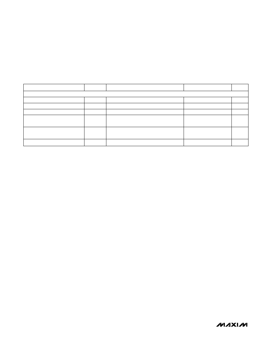
ELECTRICAL CHARACTERISTICS (continued)
(V
DD
= 3.3V, OV
DD
= 2.0V, GND = 0, REFIN = REFOUT (internal reference), C
REFOUT
= 0.1µF, C
L
≈ 5pF at digital outputs, V
IN
= -
0.5dBFS, CLKTYP = high, DCE = high, PD = low, G/T = low, f
CLK
= 65MHz (50% duty cycle), C
REFP
= C
REFN
= 0.1µF, 1µF in parallel with
10µF between REFP and REFN, C
COM
= 0.1µF in parallel with 2.2µF to GND, T
A
= -40°C to +85°C, unless otherwise noted. Typical values
are at T
A
= +25°C.) (Note 1)
PARAMETER
SYMBOL
CONDITIONS
MIN
TYP
MAX
UNITS
TIMING CHARACTERISTICS
(Figure 5)
Clock Pulse-Width High
t
CH
7.7
ns
Clock Pulse-Width Low
t
CL
7.7
ns
Data Valid Delay
t
DAV
C
L
= 5pF (Note 5)
6.4
ns
Data Setup Time Before Rising
Edge of DAV
t
SETUP
C
L
= 5pF (Notes 3, 5)
8.5
ns
Data Hold Time After Rising Edge
of DAV
t
HOLD
C
L
= 5pF (Notes 3, 5)
6.3
ns
Wake-Up Time from Power-Down
t
WAKE
V
REFIN
= 2.048V
10
ms
Note 1:
Specifications
≥+25°C guaranteed by production test, <+25°C guaranteed by design and characterization.
Note 2:
Specifications guaranteed by design and characterization. Devices tested for performance during production test.
Note 3:
Guaranteed by design and characterization.
Note 4:
During power-down, D11–D0, DOR, and DAV are high impedance.
Note 5:
Digital outputs settle to V
IH
or V
IL
.