Rainbow Electronics MAX1211 User Manual
Page 22
MAX1211
65Msps, 12-Bit, IF Sampling ADC
22
______________________________________________________________________________________
Keep the capacitive load on DAV as low as possible
(<25pF) to avoid large digital currents feeding back into
the analog portion of the MAX1211 and degrading its
dynamic performance. An external buffer on DAV isolates
it from heavy capacitive loads. Refer to the MAX1211
evaluation kit schematic for an example of DAV driving
back-end digital circuitry through an external buffer.
Data Out-of-Range Indicator (DOR)
The DOR digital output indicates when the analog input
voltage is out of range. When DOR is high, the analog
input is out of range. When DOR is low, the analog
input is within range. The valid differential input range is
from (V
REFP
- V
REFN
) to (V
REFN
- V
REFP
). Signals out-
side this valid differential range cause DOR to assert
high as shown in Table 2.
DOR is synchronized with DAV and transitions along
with output data D0–D11. There is an 8.5 clock-cycle
latency in the DOR function just as with the output data
(Figure 5).
DOR is high impedance when the MAX1211 is in
power-down (PD = high). DOR enters a high-imped-
ance state within 10ns of the rising edge of PD and
becomes active within 10ns of PD’s falling edge.
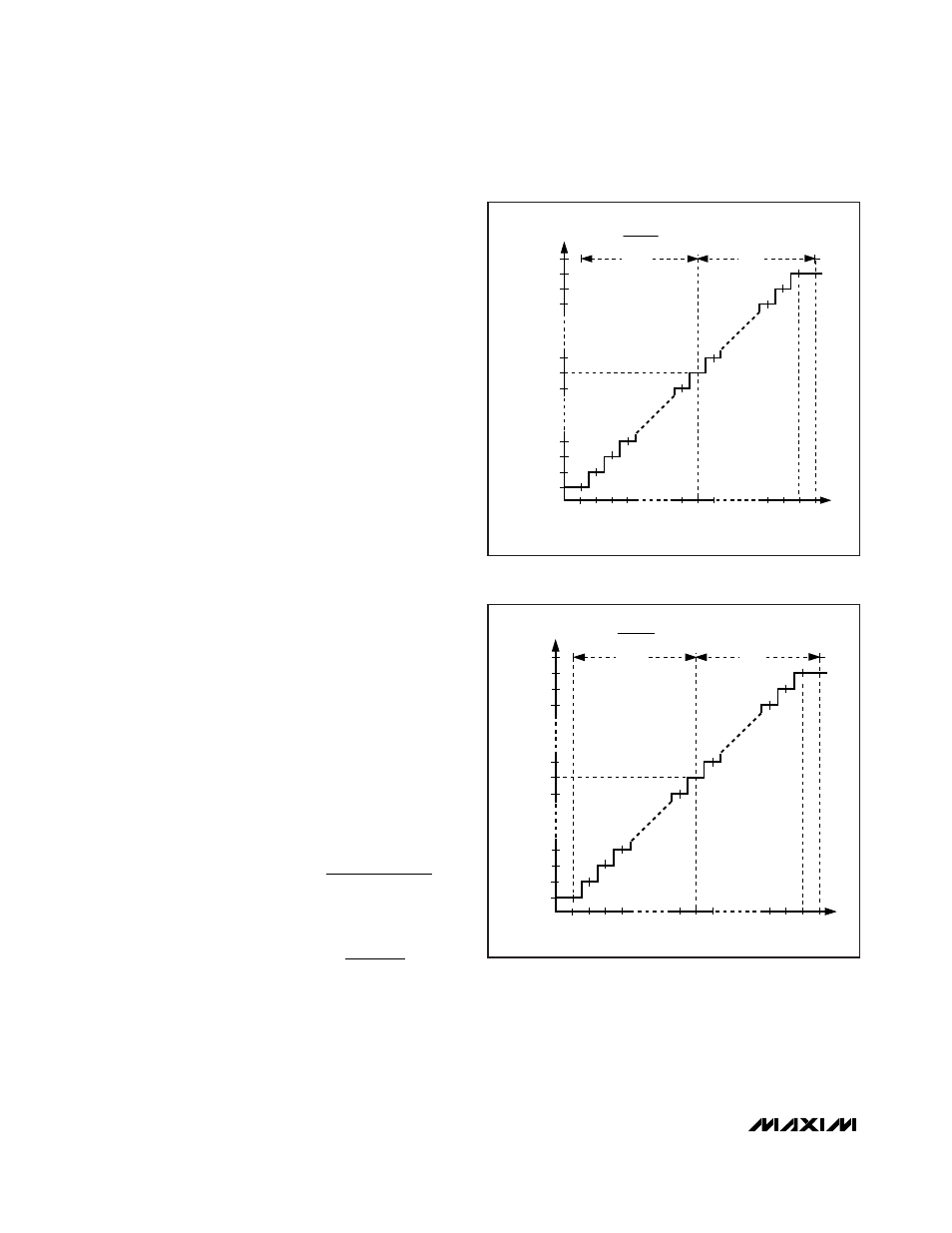
Digital Output Data (D0–D11), Output Format (G/
T
)
The MAX1211 provides a 12-bit, parallel, tri-state out-
put bus. D0–D11 and DOR update on the falling edge
of DAV and are valid on the rising edge of DAV.
The MAX1211 output data format is either Gray code or
two’s complement, depending on the logic input G/T.
With G/T high, the output data format is Gray code.
With G/T low, the output data format is two’s comple-
ment. See Figure 8 for a binary-to-Gray and Gray-to-
binary code-conversion example.
The following equations, Table 2, Figure 6, and Figure 8
define the relationship between the digital output and
the analog input:
for Gray code (G/T = 1).
for two’s complement (G/T = 0).
where CODE
10
is the decimal equivalent of the digital
output code as shown in Table 2.
The digital outputs D0–D11 are high impedance when
the MAX1211 is in power-down (PD = high). D0–D11
go high impedance within 10ns of the rising edge of PD
and become active within 10ns of PD’s falling edge.
V
V
V
V
CODE
INP
INN
REFP
REFN
−
=
−
Ч Ч
(
) 2
4096
10
V
V
V
V
CODE
INP
INN
REFP
REFN
−
=
−
Ч Ч
−
(
) 2
2048
4096
10
DIFFERENTIAL INPUT VOLTAGE (LSB)
-1
-2045
4096
2 x V
REF
1 LSB =
V
REF
= V
REFP
- V
REFN
V
REF
V
REF
0
+1
-2047
+2047
+2045
TWO'S COMPLEMENT OUTPUT CODE (LSB)
0x800
0x801
0x802
0x803
0x7FF
0x7FE
0x7FD
0xFFF
0x000
0x001
Figure 6. Two’s Complement Transfer Function (G/T = 0)
DIFFERENTIAL INPUT VOLTAGE (LSB)
-1
-2045
4096
2 x V
REF
1 LSB =
V
REF
= V
REFP
- V
REFN
V
REF
V
REF
0
+1
-2047
+2047
+2045
GRA
Y OUTPUT CODE (LSB)
0x000
0x001
0x003
0x002
0x800
0x801
0x803
0x400
0xC00
0xC01
Figure 7. Gray Code Transfer Function (G/T = 1)