Detailed description, Input track-and-hold (t/h) circuit, Reference output (refout) – Rainbow Electronics MAX1211 User Manual
Page 18
Detailed Description
The MAX1211 uses a 10-stage, fully differential,
pipelined architecture (Figure 1) that allows for high-
speed conversion while minimizing power consumption.
Samples taken at the inputs move progressively through
the pipeline stages every half clock cycle. From input to
output, the total clock-cycle latency is 8.5 clock cycles.
Each pipeline converter stage converts its input voltage
into a digital output code. At every stage, except the last,
the error between the input voltage and the digital output
code is multiplied and passed along to the next pipeline
stage. Digital error correction compensates for ADC
comparator offsets in each pipeline stage and ensures
no missing codes. Figure 2 shows the MAX1211 func-
tional diagram.
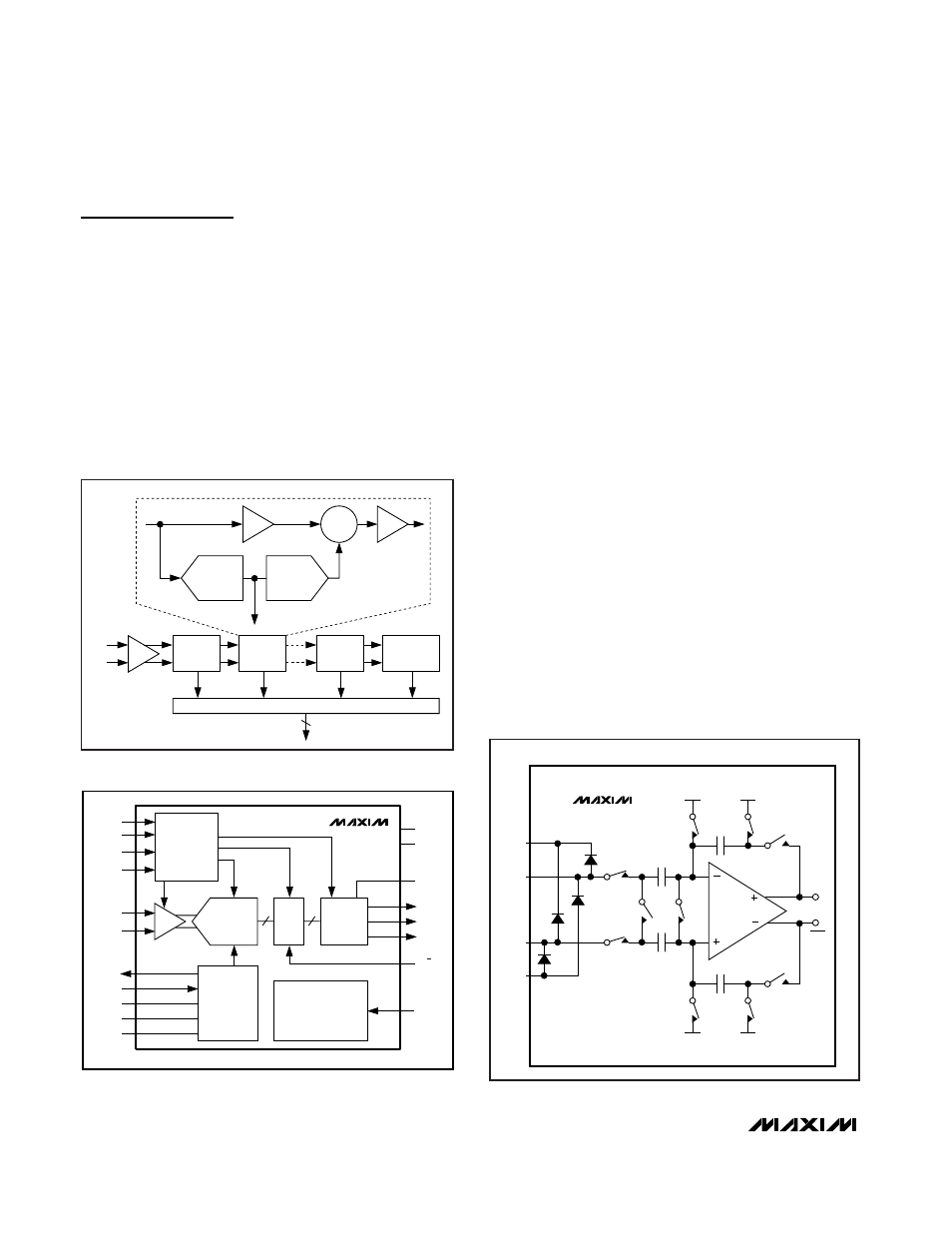
Input Track-and-Hold (T/H) Circuit
Figure 3 displays a simplified functional diagram of the
input T/H circuits. In track mode, switches S1, S2a, S2b,
S4a, S4b, S5a, and S5b are closed. The fully differential
circuits sample the input signals onto the two capacitors
(C2a and C2b) through switches S4a and S4b. S2a and
S2b set the common mode for the operational transcon-
ductance amplifier (OTA), and open simultaneously with
S1, sampling the input waveform. Switches S4a, S4b,
S5a, and S5b are then opened before switches S3a and
S3b connect capacitors C1a and C1b to the output of
the amplifier and switch S4c is closed. The resulting dif-
ferential voltages are held on capacitors C2a and C2b.
The amplifiers charge capacitors C1a and C1b to the
same values originally held on C2a and C2b. These val-
ues are then presented to the first-stage quantizers and
isolate the pipelines from the fast-changing inputs. The
wide input-bandwidth T/H amplifier allows the MAX1211
to track and sample/hold analog inputs of high frequen-
cies well beyond Nyquist. Analog input INP to INN can
be driven either differentially or single ended. For differ-
ential inputs, balance the input impedance of INP and
INN and set the common-mode voltage to midsupply
(V
DD
/ 2) for optimum performance.
Reference Output (REFOUT)
An internal bandgap reference is the basis for all the
internal voltages and bias currents used in the
MAX1211. The power-down logic input (PD) enables
and disables the reference circuit. REFOUT has
approximately 17k
Ω to GND when the MAX1211 is in
MAX1211
65Msps, 12-Bit, IF Sampling ADC
18
______________________________________________________________________________________
CLOCK
GENERATOR
AND
DUTY-CYCLE
EQUALIZER
INP
INN
12-BIT
PIPELINE
ADC
DEC
REFERENCE
SYSTEM
COM
REFOUT
REFN
REFP
OV
DD
DAV
OUTPUT
DRIVERS
D0–D11
DOR
G/T
REFIN
POWER CONTROL
AND
BIAS CIRCUITS
CLKP
CLKN
CLKTYP
PD
V
DD
GND
T/H
MAX1211
DCE
Figure 2. Functional Diagram
S3b
S3a
CML
SWITCHES SHOWN IN TRACK MODE
S5b
S5a
V
DD
INP
INN
GND
S1
OUT
OUT
C2a
C2b
S4c
S4a
S4b
C1b
C1a
INTERNAL
BIAS
INTERNAL
BIAS
CML
S2a
S2b
MAX1211
OTA
Figure 3. Internal T/H Circuit
INP
INN
STAGE 1
GAIN OF 8
4 BITS
1.5 BITS
1.5 BITS
1.5 BITS
D0–D11
1 BIT
DIGITAL ERROR CORRECTION
T/H
T/H
FLASH
ADC
DAC
x2
+
-
∑
STAGE 2
GAIN OF 2
STAGE 10
END OF PIPE
STAGE 9
GAIN OF 2
Figure 1. Pipeline Architecture—Stage Blocks