Grounding, bypassing, and board layout – Rainbow Electronics MAX1211 User Manual
Page 26
MAX1211
65Msps, 12-Bit, IF Sampling ADC
26
______________________________________________________________________________________
Grounding, Bypassing, and Board Layout
The MAX1211 requires high-speed board layout
design techniques. Refer to the MAX1211 evaluation
kit data sheet for a board layout reference. Locate all
bypass capacitors as close to the device as possible,
preferably on the same side as the ADC, using sur-
face-mount devices for minimum inductance. Bypass
V
DD
to GND with a 0.1µF ceramic capacitor in parallel
with a 2.2µF ceramic capacitor. Bypass OV
DD
to GND
with a 0.1µF ceramic capacitor in parallel with a 2.2µF
ceramic capacitor.
Multilayer boards with ample ground and power planes
produce the highest level of signal integrity. All
MAX1211 GNDs and the exposed backside paddle
must be connected to the same ground plane. The
MAX1211 relies on the exposed backside paddle con-
nection for a low-inductance ground connection. Use
multiple vias to connect the top-side ground to the bot-
tom-side ground. Isolate the ground plane from any
noisy digital system ground planes such as a DSP or
output buffer ground.
16.2k
Ω
47
Ω
+3.3V
2
2.048V
REFIN
REFP
REFN
COM
REFOUT
GND
4
2
3
5
1
1
39
38
39
38
2
3
1
2
3
1
1
µF
0.1
µF
V
DD
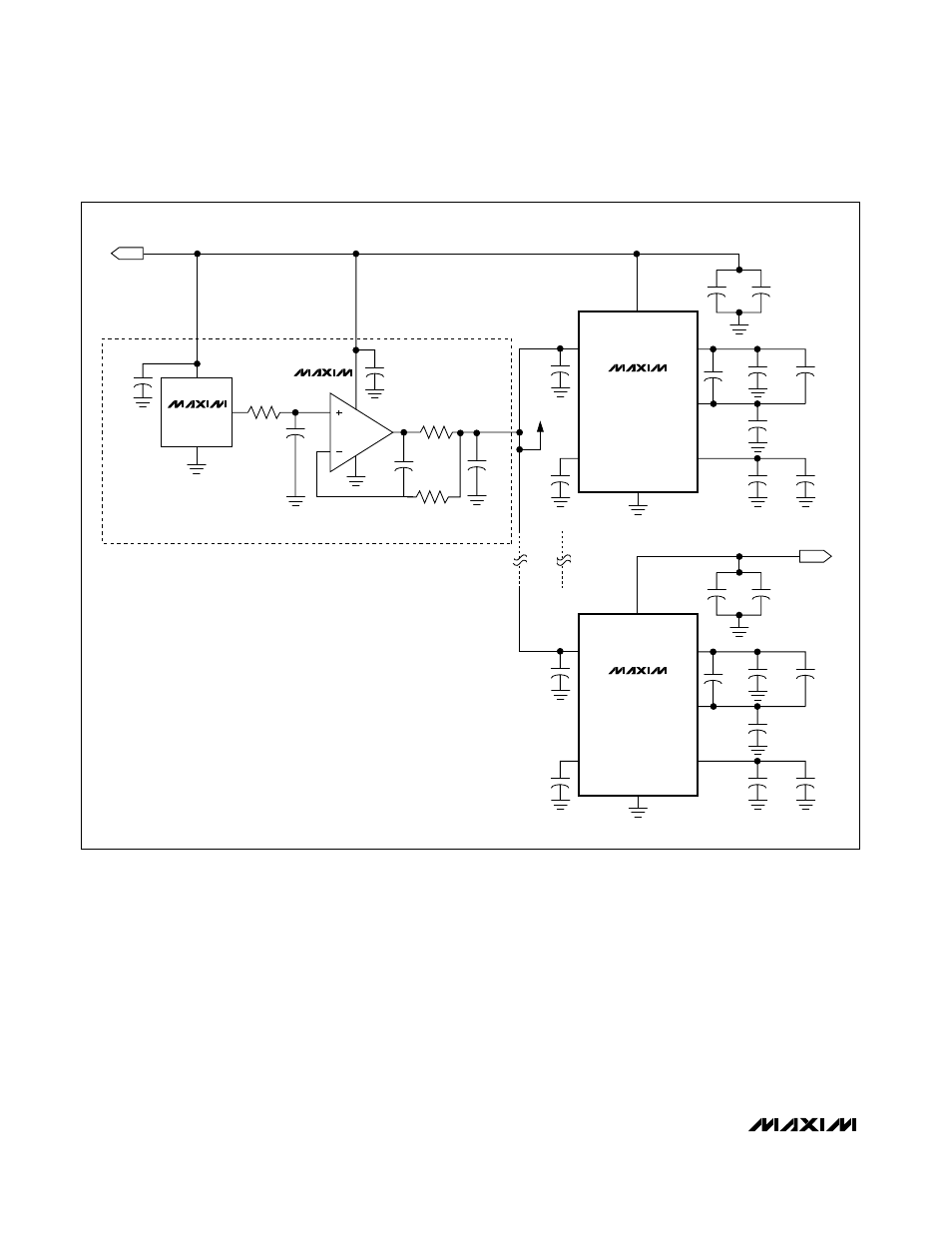
NOTE: ONE FRONT-END REFERENCE CIRCUIT PROVIDES
±15mA OF OUTPUT DRIVE.
*PLACE AS CLOSE TO THE DEVICE AS POSSIBLE.
3
0.1
µF
+3.3V
0.1
µF
2.2
µF
0.1
µF
0.1
µF
0.1
µF
0.1
µF
0.1
µF
10
µF
2.2
µF
MAX6062
MAX1211
REFIN
REFP
REFN
COM
REFOUT
GND
V
DD
0.1
µF
2.2
µF
0.1
µF
0.1
µF
*1
µF
0.1
µF
0.1
µF
0.1
µF
10
µF
2.2
µF
MAX1211
10
µF
6V
47
µF
6V
1.47k
Ω
MAX4250
*1
µF
Figure 12. External Buffered (MAX4250) Reference Drive Using a MAX6062 Bandgap Reference