Pin description, Typical operating characteristics (continued) – Rainbow Electronics MAX1211 User Manual
Page 16
MAX1211
65Msps, 12-Bit, IF Sampling ADC
16
______________________________________________________________________________________
Pin Description
PIN
NAME
FUNCTION
1
REFP
Positive Reference I/O. Conversion range is
±(V
REFP
- V
REFN
). Bypass REFP to GND with a 0.1µF
capacitor. Connect a 1µF capacitor in parallel with a 10µF capacitor between REFP and REFN.
2
REFN
Negative Reference I/O. Conversion range is
±(V
REFP
- V
REFN
). Bypass REFN to GND with a 0.1µF
capacitor. Connect a 1µF capacitor in parallel with a 10µF capacitor between REFP and REFN.
3
COM
Common-Mode Voltage I/O. Bypass COM to GND with a
≥2.2µF capacitor in parallel with a 0.1µF
capacitor.
4, 7, 16, 35
GND
Ground. Connect all ground pins and the EP together.
5
INP
Positive Analog Input. For single-ended input operation, connect signal source to INP and connect INN
to COM. For differential operation, connect the input signal between INP and INN.
6
INN
Negative Analog Input. For single-ended input operation, connect INN to COM. For differential operation,
connect the input signal between INP and INN.
8
DCE
Duty-Cycle Equalizer Input. Connect DCE low (GND) to disable the internal duty-cycle equalizer.
Connect DCE high (OVDD or VDD) to enable the internal duty-cycle equalizer.
9
CLKN
Negative Clock Input. In differential clock input mode (CLKTYP = OV
DD
or V
DD
), connect the clock
signal between CLKP and CLKN. In single-ended clock mode (CLKTYP = GND), apply the clock signal
to CLKP and tie CLKN to GND.
10
CLKP
Positive Clock Input. In differential clock input mode (CLKTYP = OV
DD
or V
DD
), connect the differential
clock signal between CLKP and CLKN. In single-ended clock mode (CLKTYP = GND), apply the single-
ended clock signal to CLKP and connect CLKN to GND.
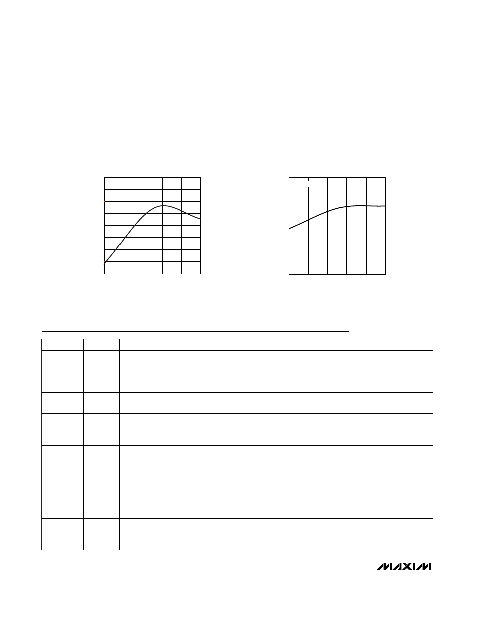
Typical Operating Characteristics (continued)
(V
DD
= 3.3V, OV
DD
= 2.0V, GND = 0, REFIN = REFOUT (internal reference), C
REFOUT
= 0.1µF, C
L
≈ 5pF at digital outputs, differential
input at -0.5dBFS, DCE = high, CLKTYP = high, PD = low, G/T = low, f
CLK
≈ 65MHz (50% duty cycle), C
REFP
= C
REFN
= 0.1µF to GND,
1µF in parallel with 10µF between REFP and REFN, C
COM
= 0.1µF in parallel with 2.2µF to GND, T
A
= +25°C, unless otherwise noted.)
OFFSET ERROR
vs. TEMPERATURE
OFFSET ERROR (%FS)
-0.06
-0.04
-0.02
0
0.04
0.02
0.06
0.08
-0.08
V
REF
= 2.048V
MAX1211 toc37
TEMPERATURE (
°C)
60
35
10
-15
-40
85
GAIN ERROR
vs. TEMPERATURE
GAIN ERROR (%FS)
0.05
0.10
0.15
0.20
0.30
0.25
0.35
0.40
0
V
REFIN
= 2.048V
MAX1211 toc38
TEMPERATURE (
°C)
60
35
10
-15
-40
85