Applications information – Rainbow Electronics MAX1211 User Manual
Page 24
MAX1211
65Msps, 12-Bit, IF Sampling ADC
24
______________________________________________________________________________________
Keep the capacitive load on the MAX1211 digital out-
puts D0–D11 as low as possible (<15pF) to avoid large
digital currents feeding back into the analog portion of
the MAX1211 and degrading its dynamic performance.
The addition of external digital buffers on the digital
outputs isolate the MAX1211 from heavy capacitive
loads. To improve the dynamic performance of the
MAX1211, add 220
Ω resistors in series with the digital
outputs close to the MAX1211. Refer to the MAX1211
EV kit schematic for an example of the digital outputs
driving a digital buffer through 220
Ω series resistors.
Power-Down Input (PD)
The MAX1211 has two power modes that are controlled
with the power-down digital input (PD). With PD low, the
MAX1211 is in its normal operating mode. With PD
high, the MAX1211 is in power-down mode.
The power-down mode allows the MAX1211 to efficient-
ly use power by transitioning to a low-power state when
conversions are not required. Additionally, the
MAX1211 parallel output bus goes high impedance in
power-down mode, allowing other devices on the bus
to be accessed.
In power-down mode, all internal circuits are off, the
analog supply current reduces to 0.045mA, and the
digital supply current reduces to 6µA. The following list
shows the state of the analog inputs and digital outputs
in power-down mode:
• INP, INN analog inputs are disconnected from the
internal input amplifier (Figure 3).
• REFOUT has approximately 17k
Ω to GND.
• REFP, COM, REFN go high impedance with respect
to V
DD
and GND, but there is an internal 4k
Ω resis-
tor between REFP and COM, as well as an internal
4k
Ω resistor between REFN and COM.
• D0–D11, DOR, and DAV go high impedance.
• CLKP, CLKN clock inputs go high impedance
(Figure 4).
The wake-up time from power-down mode is dominat-
ed by the time required to charge the capacitors at
REFP, REFN, and COM. In internal reference mode and
buffered external reference mode, the wake-up time is
typically 10ms. When operating in the unbuffered exter-
nal reference mode, the wake-up time is dependent on
the external reference drivers.
Applications Information
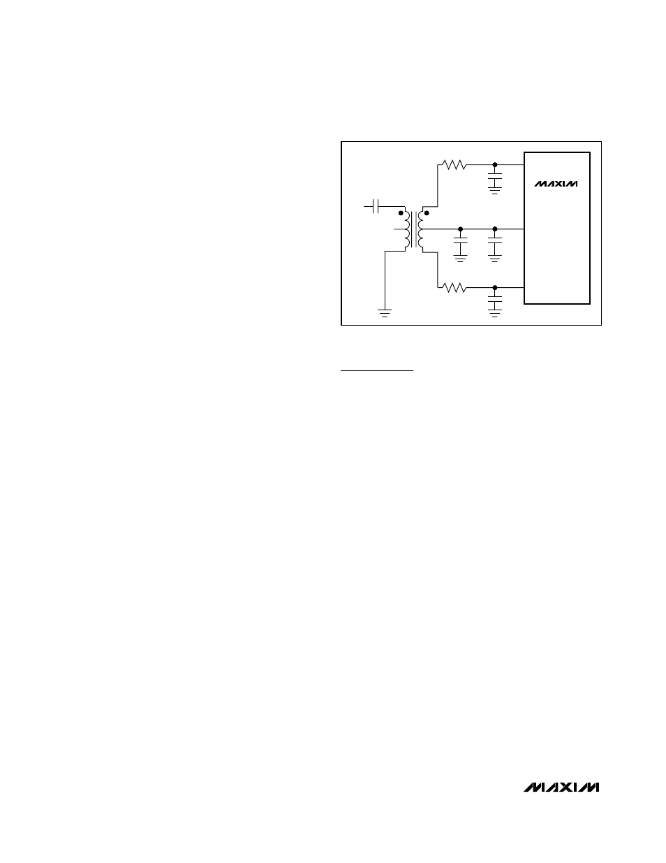
Using Transformer Coupling
In general, the MAX1211 provides better SFDR and
THD with fully differential input signals than single-
ended input drive. In differential input mode, even-
order harmonics are lower as both inputs are balanced,
and each of the ADC inputs only requires half the sig-
nal swing compared to single-ended input mode.
An RF transformer (Figure 9) provides an excellent solu-
tion to convert a single-ended input source signal to a
fully differential signal, required by the MAX1211 for opti-
mum performance. Connecting the center tap of the
transformer to COM provides a V
DD
/ 2 DC level shift to
the input. Although a 1:1 transformer is shown, a step-up
transformer can be selected to reduce the drive require-
ments. A reduced signal swing from the input driver, such
as an op amp, can also improve the overall distortion.
The configuration of Figure 9 is good for input frequen-
cies up to Nyquist (f
CLK
/ 2).
The circuit of Figure 10 converts a single-ended input
signal to fully differential just as in Figure 9. However,
Figure 10 utilizes an additional transformer to improve
the common-mode rejection, allowing high-frequency
signals beyond the Nyquist frequency. The two sets of
49.9
Ω termination resistors provide an equivalent 50Ω
termination to the signal source. The second set of ter-
mination resistors connects to COM, providing the cor-
rect input common-mode voltage. Two 0
Ω resistors in
series with the analog inputs allow high IF input fre-
quencies. These 0
Ω resistors can be replaced with low-
value resistors to limit the input bandwidth.
MAX1211
T1
N.C.
V
IN
6
1
5
2
4
3
12pF
12pF
0.1
µF
0.1
µF
2.2
µF
24.9
Ω
24.9
Ω
MINICIRCUITS
TT1-6
OR
T1-1T
INN
COM
INP
Figure 9. Transformer-Coupled Input Drive for Input
Frequencies Up to Nyquist