Single-ended ac-coupled input signal, Buffered external reference drives multiple adcs, Unbuffered external reference drives multiple adcs – Rainbow Electronics MAX1211 User Manual
Page 25
MAX1211
65Msps, 12-Bit, IF Sampling ADC
______________________________________________________________________________________
25
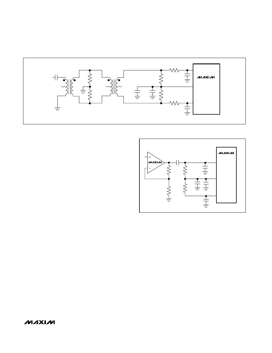
Single-Ended AC-Coupled Input Signal
Figure 11 shows an AC-coupled, single-ended input
application. The MAX4108 provides high speed, high
bandwidth, low noise, and low distortion to maintain the
input signal integrity.
Buffered External Reference Drives
Multiple ADCs
The buffered external reference mode allows for more
control over the MAX1211 reference voltage and allows
multiple converters to use a common reference. The
REFIN input impedance is >50M
Ω.
Figure 12 shows the MAX6062 precision bandgap ref-
erence used as a common reference for multiple con-
verters. The 2.048V output of the MAX6062 passes
through a one-pole, 10Hz, lowpass filter to the
MAX4250. The MAX4250 buffers the 2.048V reference
before its output is applied to the REFIN input of the
MAX1211. The MAX4250 provides a low offset voltage
(for high gain accuracy) and a low noise level.
Unbuffered External Reference Drives
Multiple ADCs
The unbuffered external reference mode allows for pre-
cise control over the MAX1211 reference and allows
multiple converters to use a common reference.
Connecting REFIN to GND disables the internal refer-
ence, allowing REFP, REFN, and COM to be driven
directly by a set of external reference sources.
Figure 13 shows the MAX6066 precision bandgap ref-
erence used as a common reference for multiple con-
verters. The 2.500V output of the MAX6066 is followed
by a 10Hz lowpass filter and precision voltage-divider.
The MAX4254 buffers the taps of this divider to provide
the +2.000V, +1.500V, and +1.000V sources to drive
REFP, REFN, and COM. The MAX4254 provides a low-
offset voltage and low-noise level. The individual volt-
age followers are connected to 10Hz lowpass filters,
which filter both the reference voltage and amplifier
noise to a level of 3nV/
√Hz. The 2.000V and 1.000V ref-
erence voltages set the differential full-scale range of
the associated ADCs at ±1.000V.
The common power supply for all active components
removes any concern regarding power-supply
sequencing when powering up or down.
With the outputs of the MAX4254 matching better than
0.1%, the buffers and subsequent lowpass support as
many as eight ADCs.
MAX1211
0.1
µF
100
Ω
100
Ω
5.6pF
5.6pF
INP
INN
COM
0.1
µF
V
IN
MAX4108
24.9
Ω
24.9
Ω
2.2
µF
Figure 11. Single-Ended, AC-Coupled Input Drive
MAX1211
T1
N.C.
V
IN
6
1
5
2
4
3
5.6pF
5.6pF
0.1
µF
0
Ω*
49.9
Ω
0.5%
49.9
Ω
0.5%
0
Ω*
MINICIRCUITS
ADT1-1WT
T1
N.C.
N.C.
6
1
5
2
4
3
MINICIRCUITS
ADT1-1WT
INP
COM
INN
*0
Ω RESISTORS CAN BE REPLACED WITH
LOW-VALUE RESISTORS TO LIMIT THE
INPUT BANDWIDTH.
0.1
µF
4.7
µF
49.9
Ω
0.5%
49.9
Ω
0.5%
Figure 10. Transformer-Coupled Input Drive for Input Frequencies Beyond Nyquist