Rainbow Electronics MAX1211 User Manual
Page 20
MAX1211
65Msps, 12-Bit, IF Sampling ADC
20
______________________________________________________________________________________
Low clock jitter is required for the specified SNR perfor-
mance of the MAX1211. Analog input sampling occurs
on the falling edge of the clock signal, requiring this
edge to have the lowest possible jitter. Jitter limits the
maximum SNR performance of any ADC according to
the following relationship:
where f
IN
represents the analog input frequency and t
J
is the total system clock jitter. Clock jitter is especially
critical for undersampling applications. For example,
assuming that clock jitter is the only noise source, to
obtain the specified 66.8dB of SNR with an input fre-
quency of 175MHz, the system must have less than
0.42ps of clock jitter. In actuality, there are other noise
sources such as thermal noise and quantization noise
that contribute to the system noise requiring the clock
jitter to be less than 0.24ps to obtain the specified
66.8dB of SNR at 175MHz.
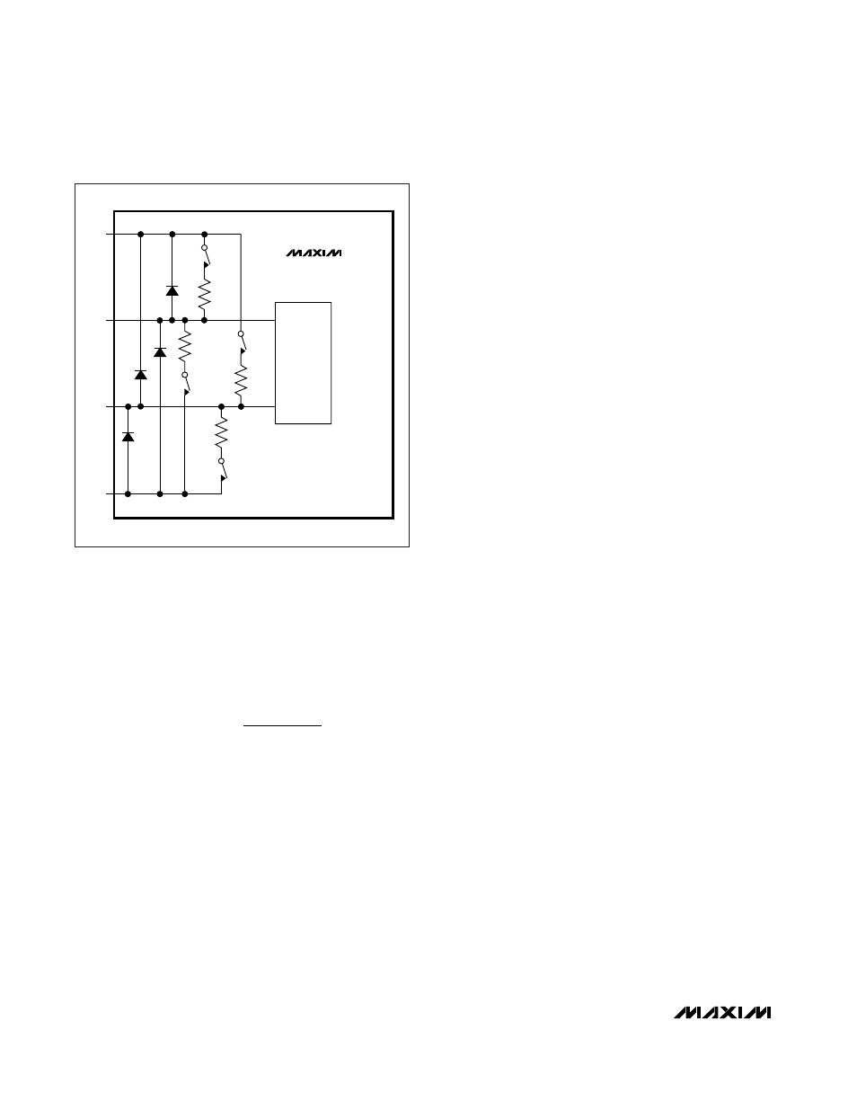
Clock Duty-Cycle Equalizer (DCE)
The MAX1211 clock duty-cycle equalizer allows for a
wide 20% to 80% clock duty cycle when enabled (DCE
= OV
DD
or V
DD
). When disabled (DCE = GND), the
MAX1211 accepts a narrow 45% to 65% clock duty
cycle. See the Typical Operating Characteristics section
for dynamic performance vs. clock duty-cycle plots.
The clock duty-cycle equalizer uses a delay-locked
loop to create internal timing signals that are duty-cycle
independent. Due to this delay-locked loop, the
MAX1211 requires approximately 100 clock cycles to
acquire and lock to new clock frequencies.
Disabling the clock duty-cycle equalizer reduces the
analog supply current by 1.5mA.
System Timing Requirements
Figure 5 shows the relationship between the clock, ana-
log inputs, DAV indicator, DOR indicator, and the result-
ing output data. The analog input is sampled on the
falling edge of the clock signal and the resulting data
appears at the digital outputs 8.5 clock cycles later.
The DAV indicator is synchronized with the digital out-
put and optimized for use in latching data into digital
back-end circuitry. Alternatively, digital back-end cir-
cuitry can be latched with the falling edge of the clock.
Data Valid Output (DAV)
DAV is a single-ended version of the input clock
(CLKP). The output data changes on the falling edge of
DAV, and DAV rises once the output data is valid.
The state of the duty-cycle equalizer input (DCE)
changes the waveform at DAV. With the duty-cycle
equalizer disabled (DCE = low), the DAV signal is the
inverse of the signal at CLKP delayed by 6.4ns. With
the duty-cycle equalizer enabled (DCE = high), the
DAV signal has a fixed pulse width that is independent
of CLKP. In either case, with DCE high or low, output
data at D0–D11 and DOR are valid from 8.5ns before
the rising edge of DAV to 6.3ns after the rising edge of
DAV, and the rising edge of DAV is synchronized to
have a 6.4ns delay from the falling edge of CLKP.
DAV is high impedance when the MAX1211 is in
power down (PD = high). DAV is capable of sinking
and sourcing 600µA and has three times the drive
strength of D0–D11 and DOR. DAV is typically used to
latch the MAX1211 output data into an external back-
end digital circuit.
SNR
f
t
IN
J
=
Ч
Ч Ч
Ч
⎛
⎝⎜
⎞
⎠⎟
20
1
2
log
π
10k
Ω
10k
Ω
10k
Ω
10k
Ω
SWITCHES S
1_
AND S
2_
ARE OPEN
DURING POWER-DOWN, MAKING
CLKP AND CLKN HIGH IMPEDANCE.
SWITCHES S
2_
ARE OPEN IN
SINGLE-ENDED CLOCK MODE.
V
DD
CLKP
CLKN
GND
S
1H
S
2H
S
1L
S
2L
DUTY-
CYCLE
EQUALIZER
MAX1211
Figure 4. Simplified Clock Input Circuit