Electrical characteristics (continued) – Rainbow Electronics MAX1211 User Manual
Page 3
MAX1211
65Msps, 12-Bit, IF Sampling ADC
_______________________________________________________________________________________
3
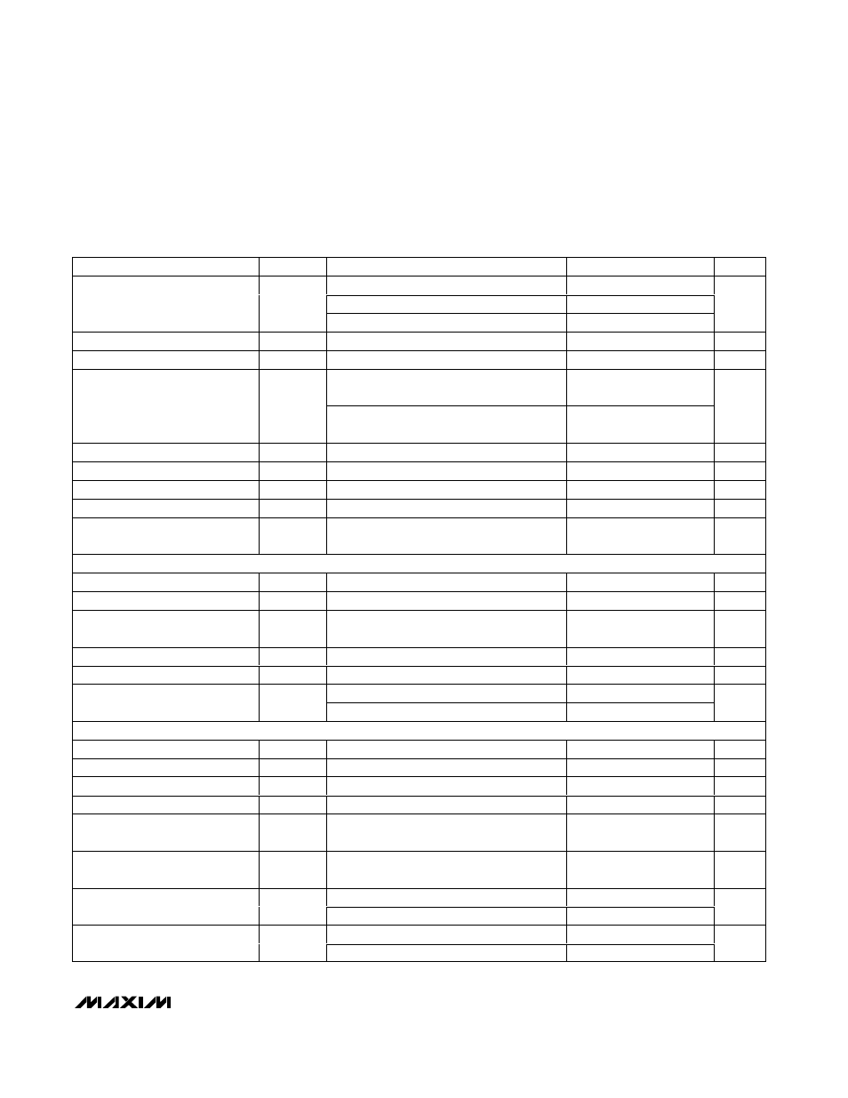
ELECTRICAL CHARACTERISTICS (continued)
(V
DD
= 3.3V, OV
DD
= 2.0V, GND = 0, REFIN = REFOUT (internal reference), C
REFOUT
= 0.1µF, C
L
≈ 5pF at digital outputs, V
IN
= -
0.5dBFS, CLKTYP = high, DCE = high, PD = low, G/T = low, f
CLK
= 65MHz (50% duty cycle), C
REFP
= C
REFN
= 0.1µF, 1µF in parallel with
10µF between REFP and REFN, C
COM
= 0.1µF in parallel with 2.2µF to GND, T
A
= -40°C to +85°C, unless otherwise noted. Typical values
are at T
A
= +25°C.) (Note 1)
PARAMETER
SYMBOL
CONDITIONS
MIN
TYP
MAX
UNITS
f
IN
= 3MHz at -0.5dBFS (Note 3)
-89.3
-80.0
f
IN
= 70MHz at -0.5dBFS (Note 3)
-81.3
-73.6
Total Harmonic Distortion
THD
f
IN
= 175MHz at -5dBFS
-78.7
-73.6
dBc
Second Harmonic
HD2
f
IN1
= 70MHz at -5dBFS
-82.4
-74.0
dBc
Third Harmonic
HD3
f
IN
= 70MHz at -0.5dBFS (Note 3)
-90.9
-84.6
dBc
f
IN1
= 68.5MHz at -7dBFS
f
IN2
= 71.5MHz at -7dBFS
-82.4
Third-Order Intermodulation
IM3
f
IN1
= 172.5MHz at -7dBFS
f
IN2
= 177.5MHz at -7dBFS
-81.2
dBc
Full-Power Bandwidth
FPBW
Input at -0.5dBFS, -3dB rolloff
700
MHz
Aperture Delay
t
AD
Figure 14
0.9
ns
Aperture Jitter
t
AJ
Figure 14
<0.2
ps
RMS
Output Noise
n
OUT
INP = INN = COM
0.5
LSB
RMS
Overdrive Recovery Time
±10% beyond full scale
1
Clock
cycles
INTERNAL REFERENCE
(REFIN = REFOUT; V
REFP
, V
REFN
, and V
COM
are generated internally)
REFOUT Output Voltage
V
REFOUT
1.996
2.048
2.071
V
COM Output Voltage
V
COM
V
DD
/ 2
1.65
V
Differential Reference Output
Voltage
V
REF
V
REF
= V
REFP
- V
REFN
1.024
V
REFOUT Load Regulation
35
mV/mA
REFOUT Temperature Coefficient
TC
REF
+100
ppm/°C
Short to V
DD
0.24
REFOUT Short-Circuit Current
Short to GND
2.1
mA
B U F F ER ED EXT ER N A L R EF ER EN C E
( RE FIN d r i ven exter nal l y, V
R E F IN
= 2.048V , V
R E F P
, V
R E F N
, and V
C OM
ar e g ener ated i nter nal l y)
REFIN Input Voltage
V
REFIN
2.048
V
REFP Output Voltage
V
REFP
(V
DD
/ 2) + (V
REFIN
/ 4)
2.162
V
REFN Output Voltage
V
REFN
(V
DD
/ 2) - (V
REFIN
/ 4)
1.138
V
COM Output Voltage
V
COM
V
DD
/ 2
1.60
1.65
1.70
V
Differential Reference Output
Voltage
V
REF
V
REF
= V
REFP
- V
REFN
0.978
1.024
1.059
V
Differential Reference
Temperature Coefficient
+12.5
ppm/°C
Source
0.4
Maximum REFP Current
I
REFP
Sink
1.4
mA
Source
1.0
Maximum REFN Current
I
REFN
Sink
1.0
mA