Unbuffered external reference drives multiple adcs, Grounding, bypassing, and board layout – Rainbow Electronics MAX1207 User Manual
Page 24
MAX1207
65Msps, 12-Bit ADC
24
______________________________________________________________________________________
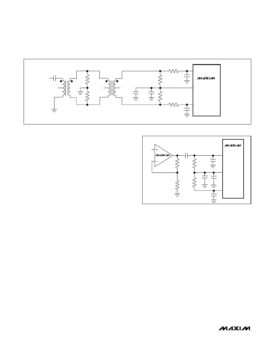
Unbuffered External Reference Drives
Multiple ADCs
The unbuffered external reference mode allows for pre-
cise control over the MAX1207 reference and allows
multiple converters to use a common reference.
Connecting REFIN to GND disables the internal refer-
ence, allowing REFP, REFN, and COM to be driven
directly by a set of external reference sources.
Figure 13 shows the MAX6066 precision bandgap ref-
erence used as a common reference for multiple con-
verters. The 2.500V output of the MAX6066 is followed
by a 10Hz lowpass filter and precision voltage-divider.
The MAX4254 buffers the taps of this divider to provide
the +2.000V, +1.500V, and +1.000V sources to drive
REFP, REFN, and COM. The MAX4254 provides a low
offset voltage and low noise level. The individual volt-
age followers are connected to 10Hz lowpass filters,
which filter both the reference voltage and amplifier
noise to a level of 3nV/√Hz. The 2.000V and 1.000V ref-
erence voltages set the differential full-scale range of
the associated ADCs at ±1.000V.
The common power supply for all active components
removes any concern regarding power-supply
sequencing when powering up or down.
With the outputs of the MAX4254 matching better than
0.1%, the buffers and subsequent lowpass support as
many as 8 ADCs.
Grounding, Bypassing, and Board Layout
The MAX1207 requires high-speed board layout design
techniques. Refer to the MAX1211 evaluation kit data
sheet for a board layout reference. Locate all bypass
capacitors as close to the device as possible, prefer-
ably on the same side as the ADC, using surface-
mount devices for minimum inductance. Bypass V
DD
to
GND with a 0.1µF ceramic capacitor in parallel with a
2.2µF ceramic capacitor. Bypass OV
DD
to GND with a
0.1µF ceramic capacitor in parallel with a 2.2µF ceram-
ic capacitor.
Multilayer boards with ample ground and power planes
produce the highest level of signal integrity. All
MAX1207 GNDs and the exposed backside paddle
must be connected to the same ground plane. The
MAX1207 relies on the exposed backside paddle con-
nection for a low-inductance ground connection. Use
multiple vias to connect the top-side ground to the bot-
tom-side ground. Isolate the ground plane from any
noisy digital system ground planes such as a DSP or
output buffer ground.
Route high-speed digital signal traces away from the
sensitive analog traces. Keep all signal lines short and
free of 90° turns.
Ensure that the differential analog input network layout
is symmetric and that all parasitics are balanced equal-
ly. Refer to the MAX1211 evaluation kit data sheet for
an example of symmetric input layout.
MAX1207
0.1µF
100Ω
100Ω
12pF
12pF
INP
INN
COM
0.1µF
V
IN
MAX4108
24.9Ω
24.9Ω
2.2µF
Figure 11. Single-Ended, AC-Coupled Input Drive
MAX1207
T1
N.C.
V
IN
6
1
5
2
4
3
12pF
12pF
0.1µF
0Ω*
49.9Ω
0.5%
49.9Ω
0.5%
0Ω*
MINICIRCUITS
ADT1-1WT
T1
N.C.
N.C.
6
1
5
2
4
3
MINICIRCUITS
ADT1-1WT
INP
COM
INN
*0Ω RESISTORS CAN BE REPLACED WITH
LOW-VALUE RESISTORS TO LIMIT THE
INPUT BANDWIDTH.
0.1µF
4.7µF
49.9Ω
0.5%
49.9Ω
0.5%
Figure 10. Transformer-Coupled Input Drive for Input Frequencies Beyond Nyquist