Rainbow Electronics MAX1207 User Manual
Page 21
MAX1207
65Msps, 12-Bit ADC
______________________________________________________________________________________
21
DOR is high impedance when the MAX1207 is in
power-down (PD = high). DOR enters a high-imped-
ance state within 10ns of the rising edge of PD and
becomes active within 10ns of PD’s falling edge.
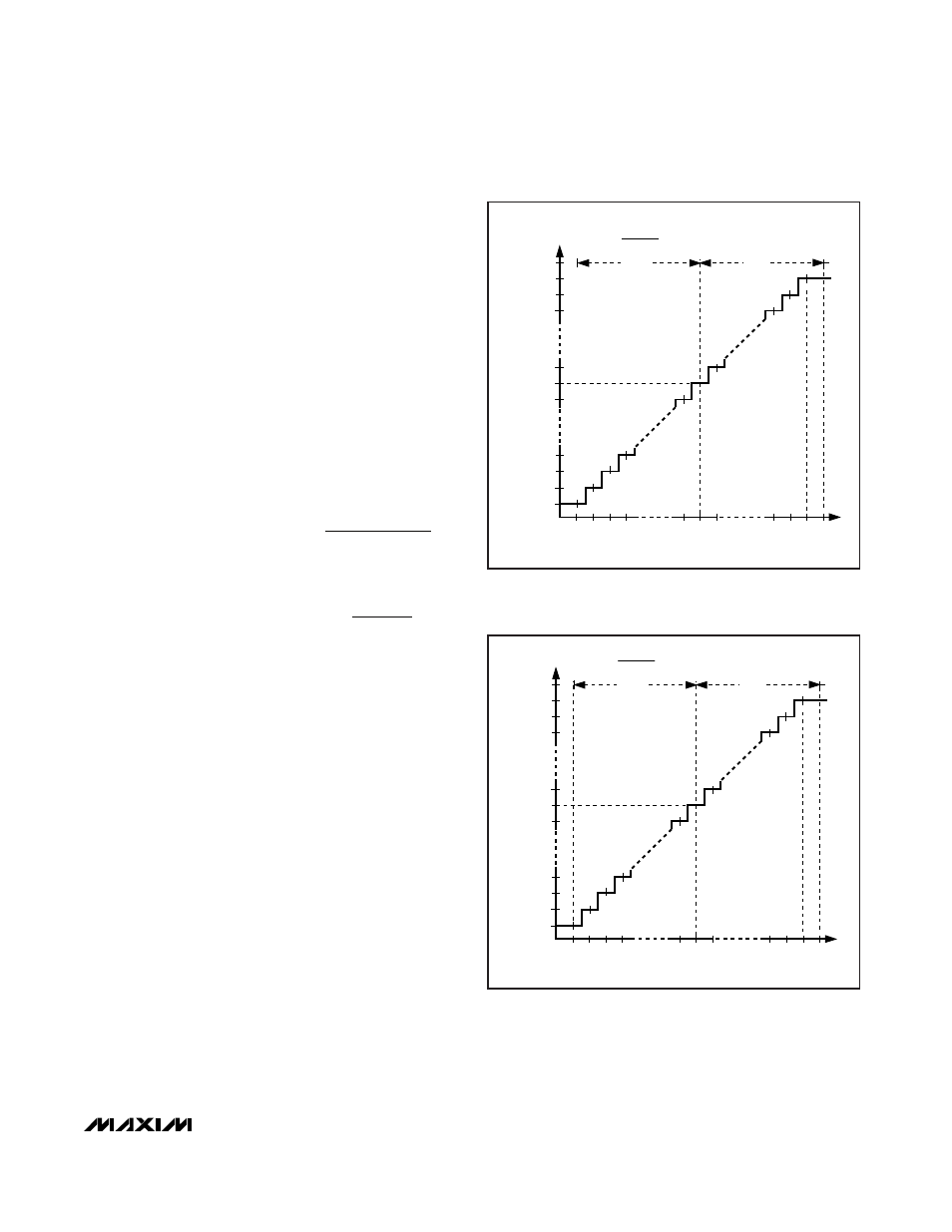
Digital Output Data (D0–D11), Output Format (G/
T
)
The MAX1207 provides a 12-bit, parallel, tri-state out-
put bus. D0–D11 and DOR update on the falling edge
of DAV and are valid on the rising edge of DAV.
The MAX1207 output data format is either Gray code or
two’s complement, depending on the logic input G/T.
With G/T high, the output data format is Gray code.
With G/T low, the output data format is two’s comple-
ment. See Figure 8 for a binary-to-Gray and Gray-to-
binary code-conversion example.
The following equations, Table 2, Figure 6, and Figure 8
define the relationship between the digital output and
the analog input:
for Gray code (G/T = 1).
for two’s complement (G/T = 0).
where CODE
10
is the decimal equivalent of the digital
output code as shown in Table 2.
The digital outputs D0–D11 are high impedance when
the MAX1207 is in power-down (PD = high). D0–D11
go high impedance within 10ns of the rising edge of PD
and become active within 10ns of PD’s falling edge.
Keep the capacitive load on the MAX1207 digital out-
puts D0–D11 as low as possible (<15pF) to avoid large
digital currents feeding back into the analog portion of
the MAX1207 and degrading its dynamic performance.
The addition of external digital buffers on the digital out-
puts isolate the MAX1207 from heavy capacitive loads.
To improve the dynamic performance of the MAX1207,
add 220Ω resistors in series with the digital outputs
close to the MAX1207. Refer to the MAX1211 evaluation
kit schematic for an example of the digital outputs dri-
ving a digital buffer through 220Ω series resistors.
Power-Down Input (PD)
The MAX1207 has two power modes that are controlled
with the power-down digital input (PD). With PD low, the
MAX1207 is in its normal operating mode. With PD
high, the MAX1207 is in power-down mode.
The power-down mode allows the MAX1207 to efficient-
ly use power by transitioning to a low-power state when
conversions are not required. Additionally, the
MAX1207 parallel output bus goes high impedance in
power-down mode, allowing other devices on the bus
to be accessed.
V
V
V
V
CODE
INP
INN
REFP
REFN
−
=
−
Ч Ч
(
) 2
4096
10
V
V
V
V
CODE
INP
INN
REFP
REFN
−
=
−
Ч Ч
−
(
) 2
2048
4096
10
DIFFERENTIAL INPUT VOLTAGE (LSB)
-1
-2045
4096
2 x V
REF
1 LSB =
V
REF
= V
REFP
- V
REFN
V
REF
V
REF
0
+1
-2047
+2047
+2045
TWO'S COMPLEMENT OUTPUT CODE (LSB)
0x800
0x801
0x802
0x803
0x7FF
0x7FE
0x7FD
0xFFF
0x000
0x001
Figure 6. Two’s Complement Transfer Function (G/T = 0)
DIFFERENTIAL INPUT VOLTAGE (LSB)
-1
-2045
4096
2 x V
REF
1 LSB =
V
REF
= V
REFP
- V
REFN
V
REF
V
REF
0
+1
-2047
+2047
+2045
GRA
Y OUTPUT CODE (LSB)
0x000
0x001
0x003
0x002
0x800
0x801
0x803
0x400
0xC00
0xC01
Figure 7. Gray Code Transfer Function (G/T = 1)