Pin description (continued) – Rainbow Electronics MAX1207 User Manual
Page 16
MAX1207
65Msps, 12-Bit ADC
16
______________________________________________________________________________________
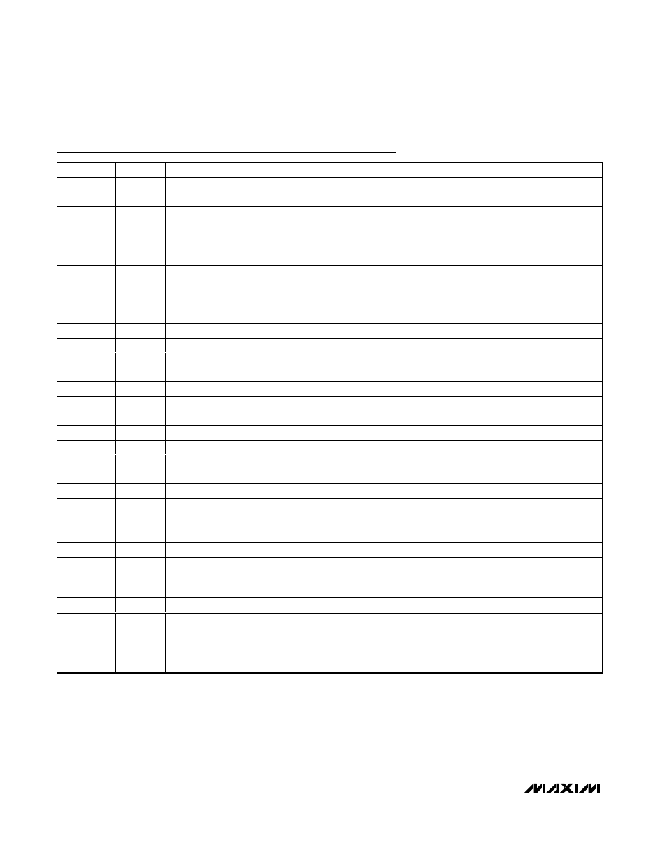
Pin Description (continued)
PIN
NAME
FUNCTION
11
CLKTYP
Clock Type Definition Input. Connect CLKTYP to GND to define the single-ended clock input. Connect
CLKTYP to OV
DD
or V
DD
to define the differential clock input.
12–15, 36
V
DD
Analog Power Input. Connect V
DD
to a 3.0V to 3.6V power supply. Bypass V
DD
to GND with a parallel
capacitor combination of ≥2.2µF and 0.1µF. Connect all V
DD
pins to the same potential.
17, 34
OV
DD
Output Driver Power Input. Connect OV
DD
to a 1.7V to V
DD
power supply. Bypass OV
DD
to GND with a
parallel capacitor combination of ≥2.2µF and 0.1µF.
18
DOR
Data Out-of-Range Indicator. The DOR digital output indicates when the analog input voltage is out of
range. When DOR is high, the analog input is beyond its full-scale range. When DOR is low, the analog
input is within its full-scale range.
19
D11
CMOS Digital Output, Bit 11 (MSB)
20
D10
CMOS Digital Output, Bit 10
21
D9
CMOS Digital Output, Bit 9
22
D8
CMOS Digital Output, Bit 8
23
D7
CMOS Digital Output, Bit 7
24
D6
CMOS Digital Output, Bit 6
25
D5
CMOS Digital Output, Bit 5
26
D4
CMOS Digital Output, Bit 4
27
D3
CMOS Digital Output, Bit 3
28
D2
CMOS Digital Output, Bit 2
29
D1
CMOS Digital Output, Bit 1
30
D0
CMOS Digital Output, Bit 0 (LSB)
31, 32
I. C.
Internally Connected. Leave I. C. unconnected.
33
DAV
Data Valid Output. The DAV is a single-ended version of the input clock that is compensated to correct
for any input clock duty-cycle variations. The MAX1211 evaluation kit (MAX1211EVKIT) utilizes DAV to
latch data (D0–D11) into external back-end digital circuitry.
37
PD
Power-Down Input. Force PD high for power-down mode. Force PD low for normal operation.
38
REFOUT
Internal Reference Voltage Output. For internal reference operation, connect REFOUT directly to REFIN
or use a resistive-divider from REFOUT to set the voltage at REFIN. Bypass REFOUT to GND with a
≥0.1µF capacitor.
39
REFIN
Reference Input. V
REFIN
= 2 x (V
REFP
- V
REFN
). Bypass REFIN to GND with a ≥0.1µF capacitor.
40
G/T
Output Format Select Input. Connect G/T to GND for the two’s complement digital output format. Connect
G/T to OV
DD
or V
DD
for the Gray code digital output format.
—
EP
Exposed Paddle. EP is internally connected to GND. Externally connect EP to GND to achieve specified
performance.