Applications information – Rainbow Electronics MAX1207 User Manual
Page 23
MAX1207
65Msps, 12-Bit ADC
______________________________________________________________________________________
23
In power-down mode, all internal circuits are off, the
analog supply current reduces to 0.045A, and the digi-
tal supply current reduces to 6µA. The following list
shows the state of the analog inputs and digital outputs
in power-down mode:
• INP, INN analog inputs are disconnected from the
internal input amplifier (Figure 3).
• REFOUT has approximately 17kΩ to GND.
• REFP, COM, REFN go high impedance with respect
to V
DD
and GND, but there is an internal 4kΩ resis-
tor between REFP and COM, as well as an internal
4kΩ resistor between REFN and COM.
• D0–D11, DOR, and DAV go high impedance.
• CLKP, CLKN clock inputs go high impedance
(Figure 4).
The wake-up time from power-down mode is dominat-
ed by the time required to charge the capacitors at
REFP, REFN, and COM. In internal reference mode and
buffered external reference mode, the wake-up time is
typically 10ms. When operating in the unbuffered exter-
nal reference mode, the wake-up time is dependent on
the external reference drivers.
Applications Information
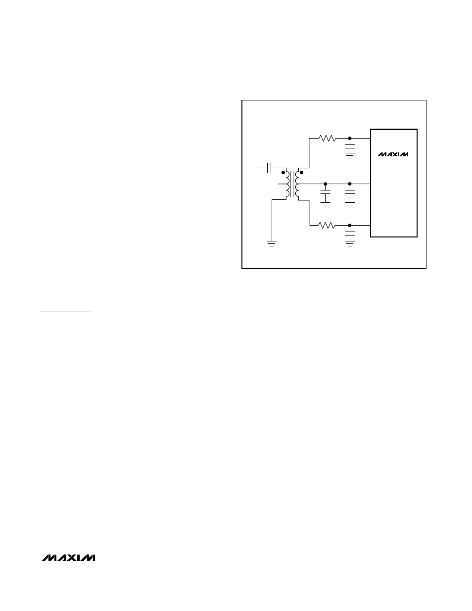
Using Transformer Coupling
In general, the MAX1207 provides better SFDR and
THD with fully differential input signals than single-
ended input drive. In differential input mode, even-
order harmonics are lower as both inputs are balanced,
and each of the ADC inputs only requires half the sig-
nal swing compared to single-ended input mode.
An RF transformer (Figure 9) provides an excellent
solution to convert a single-ended input source signal
to a fully differential signal, required by the MAX1207
for optimum performance. Connecting the center tap of
the transformer to COM provides a V
DD
/ 2 DC level
shift to the input. Although a 1:1 transformer is shown, a
step-up transformer can be selected to reduce the
drive requirements. A reduced signal swing from the
input driver, such as an op amp, can also improve the
overall distortion. The configuration of Figure 9 is good
for input frequencies up to Nyquist (f
CLK
/ 2).
The circuit of Figure 10 converts a single-ended input
signal to fully differential just as in Figure 9. However,
Figure 10 utilizes an additional transformer to improve
the common-mode rejection, allowing high-frequency
signals beyond the Nyquist frequency. The two sets of
49.9Ω termination resistors provide an equivalent 50Ω
termination to the signal source. The second set of ter-
mination resistors connects to COM, providing the cor-
rect input common-mode voltage. Two 0Ω resistors in
series with the analog inputs allow high IF input fre-
quencies. These 0Ω resistors can be replaced with low-
value resistors to limit the input bandwidth.
Single-Ended AC-Coupled Input Signal
Figure 11 shows an AC-coupled, single-ended input
application. The MAX4108 provides high speed, high
bandwidth, low noise, and low distortion to maintain the
input signal integrity.
Buffered External Reference Drives
Multiple ADCs
The buffered external reference mode allows for more
control over the MAX1207 reference voltage and allows
multiple converters to use a common reference. The
REFIN input impedance is >50MΩ.
Figure 12 shows the MAX6062 precision bandgap ref-
erence used as a common reference for multiple con-
verters. The 2.048V output of the MAX6062 passes
through a one-pole 10Hz lowpass filter to the MAX4250.
The MAX4250 buffers the 2.048V reference before its
output is applied to the REFIN input of the MAX1207.
The MAX4250 provides a low offset voltage (for high
gain accuracy) and a low noise level.
MAX1207
T1
N.C.
V
IN
6
1
5
2
4
3
12pF
12pF
0.1µF
0.1µF
2.2µF
24.9Ω
24.9Ω
MINICIRCUITS
TT1-6
OR
T1-1T
INN
COM
INP
Figure 9. Transformer-Coupled Input Drive for Input
Frequencies Up to Nyquist