Table 1. reference modes – Rainbow Electronics MAX1207 User Manual
Page 18
MAX1207
65Msps, 12-Bit ADC
18
______________________________________________________________________________________
Reference Output (REFOUT)
An internal bandgap reference is the basis for all the
internal voltages and bias currents used in the
MAX1207. The power-down logic input (PD) enables
and disables the reference circuit. REFOUT has
approximately 17kΩ to GND when the MAX1207 is in
power-down. The reference circuit requires 10ms to
power up and settle when power is applied to the
MAX1207 or when PD transitions from high to low.
The internal bandgap reference and buffer generate
REFOUT to be 2.048V with a +100ppm/°C temperature
coefficient. Connect an external ≥0.1µF bypass capaci-
tor from REFOUT to GND for stability. REFOUT sources
up to 1.4mA and sinks up to 100µA for external circuits
with a load regulation of 35mV/mA. Short-circuit protec-
tion limits I
REFOUT
to a 2.1mA source current when
shorted to GND and a 240µA sink current when shorted
to V
DD
.
Analog Inputs and Reference
Configurations
The MAX1207 full-scale analog input range is ±V
REF
with a common-mode input range of V
DD
/ 2 ±0.8V.
V
REF
is the difference between V
REFP
and V
REFN
. The
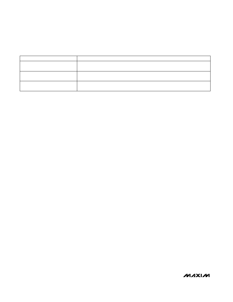
MAX1207 provides three modes of reference operation.
The voltage at REFIN (V
REFIN
) sets the reference oper-
ation mode (Table 1).
To operate the MAX1207 with the internal reference, con-
nect REFOUT to REFIN either with a direct short or
through a resistive-divider. In this mode, COM, REFP, and
REFN are low-impedance outputs with V
COM
= V
DD
/ 2,
V
REFP
= V
DD
/ 2 + V
REFIN
/ 4, and V
REFN
= V
DD
/ 2 -
V
REFIN
/ 4. The REFIN input impedance is very large
(>50MΩ). When driving REFIN through a resistive-divider,
use resistances ≥10kΩ to avoid loading REFOUT.
Buffered external reference mode is virtually identical to
internal reference mode except that the reference
source is derived from an external reference and not
the MAX1207 REFOUT. In buffered external reference
mode, apply a stable 0.7V to 2.3V source at REFIN.
COM, REFP, and REFN are low-impedance outputs
with V
COM
= V
DD
/ 2, V
REFP
= V
DD
/ 2 + V
REFIN
/ 4, and
V
REFN
= V
DD
/ 2 - V
REFIN
/ 4.
To operate the MAX1207 in unbuffered external refer-
ence mode, connect REFIN to GND. Connecting REFIN
to GND deactivates the on-chip reference buffers for
COM, REFP, and REFN. With their buffers deactivated,
COM, REFP, and REFN inputs must be driven through
separate, external reference sources. Drive V
COM
to
V
DD
/ 2 ±5%, and drive REFP and REFN such that
V
COM
= (V
REFP
+ V
REFN
) / 2. The analog input range is
±(V
REFP
- V
REFN
).
All three modes of reference operation require the same
bypass capacitor combination. Bypass COM with a
0.1µF capacitor in parallel with a ≥2.2µF capacitor to
GND. Bypass REFP and REFN each with a 0.1µF capac-
itor to GND. Bypass REFP to REFN with a 1µF capacitor
in parallel with a 10µF capacitor. Place the 1µF capacitor
as close to the device as possible. Bypass REFIN and
REFOUT to GND with a 0.1µF capacitor.
For detailed circuit suggestions, see Figures 12 and 13.
Clock Input and Clock Control Lines
(CLKP, CLKN, CLKTYP, DCE)
The MAX1207 accepts both differential and single-
ended clock inputs. For single-ended clock input opera-
tion, connect CLKTYP to GND, CLKN to GND, and drive
CLKP with the external single-ended clock signal. For
differential clock input operation, connect CLKTYP to
OV
DD
or V
DD
and drive CLKP and CLKN with the exter-
nal differential clock signal. To reduce clock jitter, the
external single-ended clock must have sharp falling
edges. Consider the clock input as an analog input and
route it away from any other analog inputs and digital
signal lines.
CLKP and CLKN are high impedance when the
MAX1207 is powered down (Figure 4).
Low clock jitter is required for the specified SNR perfor-
mance of the MAX1207. Analog input sampling occurs
on the falling edge of the clock signal, requiring this
V
REFIN
REFERENCE MODE
35% V
REFOUT
to 100% V
REFOUT
In t e r n a l re f e r e n c e m o d e . RE FIN i s d r i ven b y RE FOU T ei ther thr oug h a d i r ect shor t or a r esi sti ve
d i vi d er . V
C OM
= V
D D
/ 2, V
RE F P
= V
D D
/ 2 + V
RE F IN
/ 4, and V
RE F N
= V
D D
/ 2 - V
RE F IN
/ 4.
0.7V to 2.3V
Buffered external reference mode. An external 0.7V to 2.3V reference voltage is applied
to REFIN. V
COM
= V
DD
/ 2, V
REFP
= V
DD
/ 2 + V
REFIN
/ 4, and V
REFN
= V
DD
/ 2 - V
REFIN
/ 4.
<0.5V
Unbuffered external reference mode. REFP, REFN, and COM are driven by external
reference sources. V
REF
is the difference between the externally applied V
REFP
and V
REFN
.
Table 1. Reference Modes