Pin description (continued) – Rainbow Electronics MAX188 User Manual
Page 7
Digital Ground
Positive Supply Voltage, +5V ±5%
MAX186/MAX188
Low-Power, 8-Channel,
Serial 12-Bit ADCs
_______________________________________________________________________________________
7
PIN
NAME
FUNCTION
12
REFADJ
13
AGND
Analog Ground. Also IN- Input for single-ended conversions.
14
DGND
15
DOUT
Serial Data Output. Data is clocked out at the falling edge of SCLK. High impedance when
CS is high.
16
SSTRB
17
DIN
18
CS
19
SCLK
Input to the Reference-Buffer Amplifier. To disable the reference-buffer amplifier, tie REFADJ to
V
DD
.
Serial Clock Input. Clocks data in and out of serial interface. In external clock mode, SCLK also sets
the conversion speed. (Duty cycle must be 40% to 60% in external clock mode.)
Serial Strobe Output. In internal clock mode, SSTRB goes low when the MAX186/MAX188 begin the
A/D conversion and goes high when the conversion is done. In external clock mode, SSTRB pulses
high for one clock period before the MSB decision. High impedance when
CS is high (external mode).
Active-Low Chip Select. Data will not be clocked into DIN unless
CS is low. When CS is high, DOUT
is high impedance.
Serial Data Input. Data is clocked in at the rising edge of SCLK.
20
V
DD
+5V
3k
C
LOAD
DGND
DOUT
C
LOAD
DGND
3k
DOUT
a. High-Z to V
OH
and V
OL
to V
OH
b. High-Z to V
OL
and V
OH
to V
OL
+5V
3k
C
LOAD
DGND
DOUT
C
LOAD
DGND
3k
DOUT
a V
OH
to High-Z
b V
OL
to High-Z
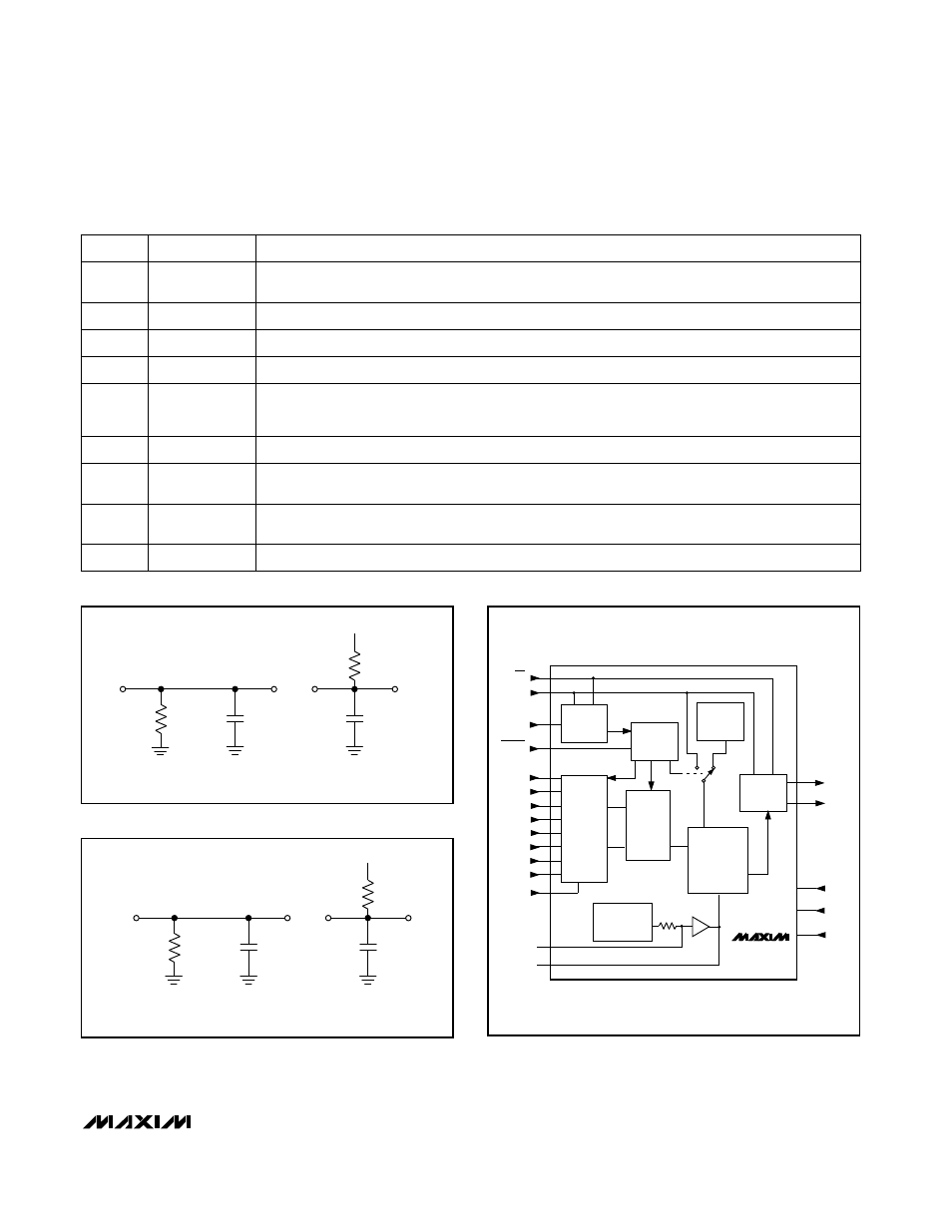
Figure 1. Load Circuits for Enable Time
Figure 2. Load Circuits for Disabled Time
INPUT
SHIFT
REGISTER
CONTROL
LOGIC
INT
CLOCK
OUTPUT
SHIFT
REGISTER
+2.46V
REFERENCE
(MAX186)
T/H
ANALOG
INPUT
MUX
12-BIT
SAR
ADC
IN
DOUT
SSTRB
V
DD
DGND
V
SS
SCLK
DIN
CH0
CH1
CH3
CH2
CH7
CH6
CH5
CH4
AGND
REFADJ
VREF
OUT
REF
CLOCK
+4.096V
20k
≈
1.65
1
2
3
4
5
6
7
8
10
11
12
13
15
16
17
18
19
MAX186
MAX188
CS
SHDN
A
20
14
9
Figure 3. Block Diagram
________________________________________________Pin Description (continued)