Electrical characteristics (continued) – Rainbow Electronics MAX188 User Manual
Page 3
External Clock Frequency Range
MAX186/MAX188
Low-Power, 8-Channel,
Serial 12-Bit ADCs
_______________________________________________________________________________________
3
PARAMETER
SYMBOL
CONDITIONS
MIN
TYP
MAX
UNITS
Small-Signal Bandwidth
-3dB rolloff
4.5
MHz
Full-Power Bandwidth
800
kHz
Internal clock
5.5
10
Conversion Time (Note 5)
t
CONV
External clock, 2MHz, 12 clocks/conversion
6
µs
Track/Hold Acquisition Time
t
AZ
1.5
µs
Aperture Delay
10
ns
Aperture Jitter
<50
ps
Internal Clock Frequency
1.7
MHz
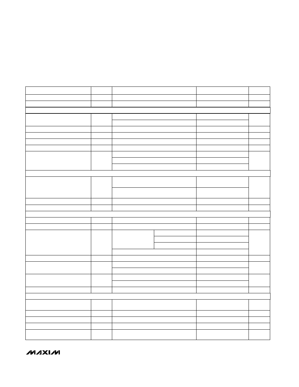
ELECTRICAL CHARACTERISTICS (continued)
(V
DD
= 5V ±5%; V
SS
= 0V or -5V; f
CLK
= 2.0MHz, external clock (50% duty cycle); 15 clocks/conversion cycle (133ksps); MAX186—
4.7µF capacitor at VREF pin; MAX188—external reference, VREF = 4.096V applied to VREF pin; T
A
= T
MIN
to T
MAX
, unless otherwise
noted.)
External compensation, 4.7µF
0.1
2.0
Internal compensation (Note 6)
0.1
0.4
Used for data transfer only
10
MHz
Unipolar, V
SS
= 0V
Input Voltage Range,
Single-Ended and Differential
(Note 9)
Bipolar, V
SS
= -5V
V
Multiplexer Leakage Current
On/off leakage current, V
IN
= ±5V
±0.01
±1
µA
Input Capacitance
(Note 6)
16
pF
VREF Output Voltage
T
A
= +25°C
4.076
4.096
4.116
V
VREF Short-Circuit Current
30
mA
MAX186A, MAX186B,
MAX186C
±30
±50
±30
±60
±30
±80
VREF Tempco
MAX186D
±30
ppm/°C
Load Regulation (Note 7)
0mA to 0.5mA output load
2.5
mV
Internal compensation
0
Capacitive Bypass at VREF
External compensation
4.7
µF
Internal compensation
0.01
Capacitive Bypass at REFADJ
External compensation
0.01
µF
MAX186_C
MAX186_E
MAX186_M
REFADJ Adjustment Range
±1.5
%
±VREF/2
0 to
VREF
Input Voltage Range
V
Input Current
200
350
µA
Input Resistance
12
20
k
Ω
Shutdown VREF Input Current
1.5
10
µA
Buffer Disable Threshold REFADJ
V
DD
-
50mV
V
V
DD
+
2.50
50mV
CONVERSION RATE
ANALOG INPUT
INTERNAL REFERENCE
(MAX186 only, reference buffer enabled)
EXTERNAL REFERENCE AT VREF
(Buffer disabled, VREF = 4.096V)