Rainbow Electronics MAX188 User Manual
Page 15
Power-Down
Choosing Power-Down Mode
You can save power by placing the converter in a
low-current shutdown state between conversions.
Select full power-down or fast power-down mode via
bits 7 and 8 of the DIN control byte with
SHDN high or
floating (see Tables 2 and 6). Pull
SHDN low at any time
to shut down the converter completely.
SHDN overrides
bits 7 and 8 of DIN word (see Table 7).
Full power-down mode turns off all chip functions that draw
quiescent current, reducing I
DD
and I
SS
typically to 2µA.
Fast power-down mode turns off all circuitry except the
bandgap reference. With the fast power-down mode, the
supply current is 30µA. Power-up time can be shortened
to 5µs in internal compensation mode.
In both software shutdown modes, the serial interface
remains operational, however, the ADC will not convert.
Table 5 illustrates how the choice of reference-buffer
compensation and power-down mode affects both
power-up delay and maximum sample rate.
In external compensation mode, the power-up time is
20ms with a 4.7µF compensation capacitor (200ms with
a 33µF capacitor) when the capacitor is fully discharged.
In fast power-down, you can eliminate start-up time by
using low-leakage capacitors that will not discharge
more than 1/2LSB while shut down. In shutdown, the
capacitor has to supply the current into the reference
(1.5µA typ) and the transient currents at power-up.
Figures 12a and 12b illustrate the various power-down
sequences in both external and internal clock modes.
Software Power-Down
Software power-down is activated using bits PD1 and
PD0 of the control byte. As shown in Table 6, PD1 and
PD0 also specify the clock mode. When software shut-
down is asserted, the ADC will continue to operate in
the last specified clock mode until the conversion is
complete. Then the ADC powers down into a low quies-
cent-current state. In internal clock mode, the interface
remains active and conversion results may be clocked
out while the MAX186/MAX188 have already entered a
software power-down.
The first logical 1 on DIN will be interpreted as a start
bit, and powers up the MAX186/MAX188. Following the
start bit, the data input word or control byte also deter-
mines clock and power-down modes. For example, if
the DIN word contains PD1 = 1, then the chip will
remain powered up. If PD1 = 0, a power-down will
resume after one conversion.
MAX186/MAX188
Low-Power, 8-Channel,
Serial 12-Bit ADCs
______________________________________________________________________________________
15
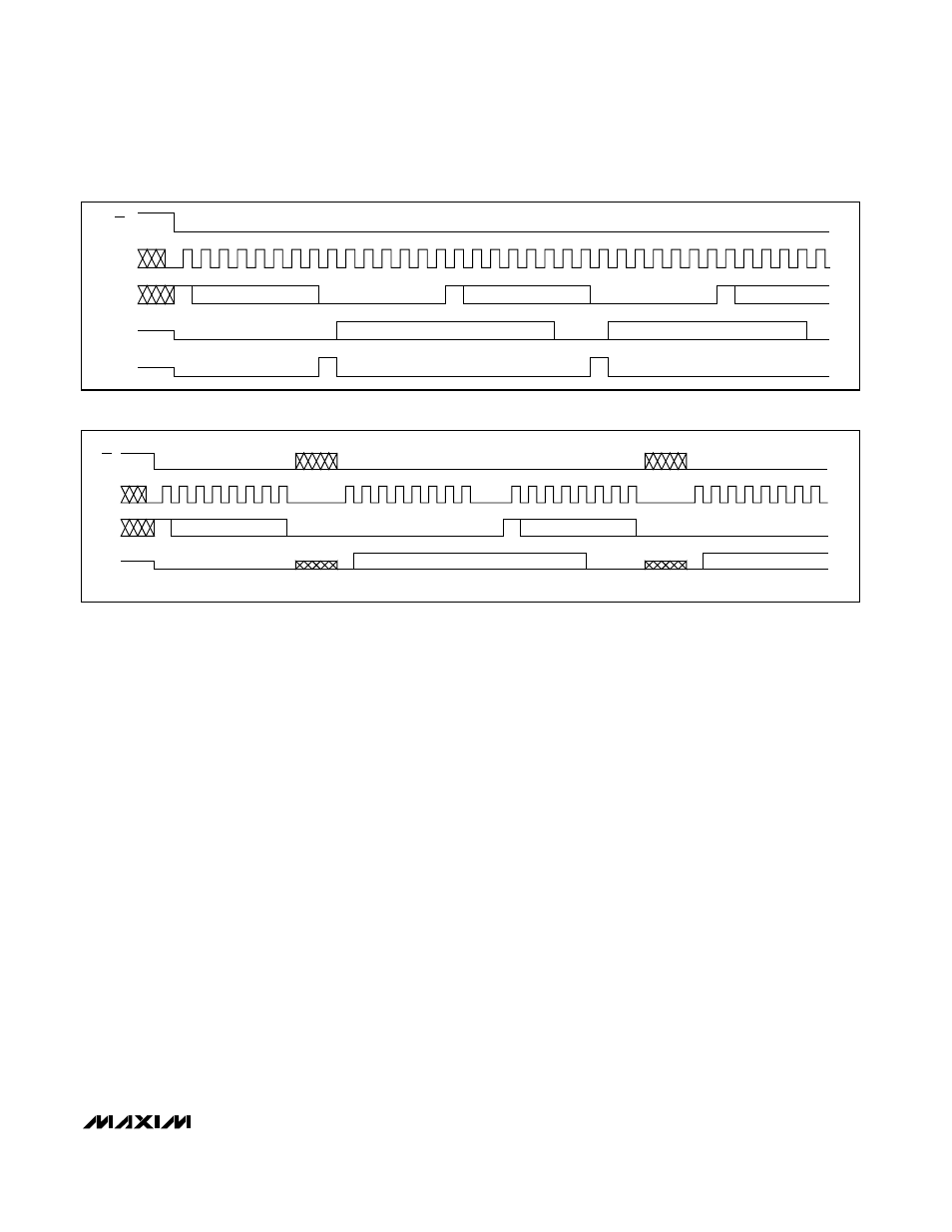
SCLK
DIN
DOUT
CS
S
CONTROL BYTE 0
CONTROL BYTE 1
S
CONVERSION RESULT 0
B11 B10 B9 B8 B7 B6 B5 B4 B3 B2 B1 B0
CONVERSION RESULT 1
SSTRB
B11 B10 B9 B8 B7 B6 B5 B4 B3 B2 B1 B0
CONTROL BYTE 2
S
1
8
1
8
1
CS
SCLK
DIN
DOUT
S
CONTROL BYTE 0
CONTROL BYTE 1
S
CONVERSION RESULT 0
B11 B10 B9 B8 B7 B6 B5 B4 B3 B2 B1 B0
B11 B10 B9 B8
CONVERSION RESULT 1
• • •
• • •
• • •
• • •
Figure 11a. External Clock Mode, 15 Clocks/Conversion Timing
Figure 11b. External Clock Mode, 16 Clocks/Conversion Timing