Rainbow Electronics MAX188 User Manual
Page 19
Using the buffered REFADJ input avoids external
buffering of the reference. To use the direct VREF input,
disable the internal buffer by tying REFADJ to V
DD
.
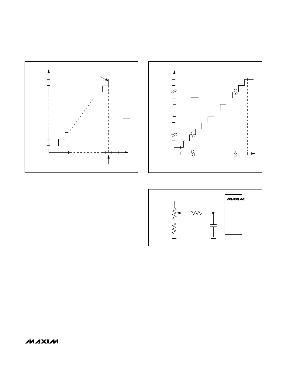
Transfer Function and Gain Adjust
Figure 15 depicts the nominal, unipolar input/output
(I/O) transfer function, and Figure 16 shows the bipolar
input/output transfer function. Code transitions occur
halfway between successive integer LSB values. Output
coding is binary with 1 LSB = 1.00mV (4.096V/4096) for
unipolar operation and 1 LSB = 1.00mV ((4.096V/2 -
-4.096V/2)/4096) for bipolar operation.
Figure 17, the MAX186 Reference-Adjust Circuit, shows
how to adjust the ADC gain in applications that use the
internal reference. The circuit provides ±1.5%
(±65LSBs) of gain adjustment range.
Layout, Grounding, Bypassing
For best performance, use printed circuit boards.
Wire-wrap boards are not recommended. Board layout
should ensure that digital and analog signal lines are
separated from each other. Do not run analog and digi-
tal (especially clock) lines parallel to one another, or
digital lines underneath the ADC package.
Figure 18 shows the recommended system ground
connections. A single-point analog ground (“star”
ground point) should be established at AGND, sepa-
rate from the logic ground. All other analog grounds
and DGND should be connected to this ground. No
other digital system ground should be connected to
this single-point analog ground. The ground return to
the power supply for this ground should be low imped-
ance and as short as possible for noise-free operation.
High-frequency noise in the V
DD
power supply may
affect the high-speed comparator in the ADC. Bypass
these supplies to the single-point analog ground with
0.1µF and 4.7µF bypass capacitors close to the
MAX186/MAX188. Minimize capacitor lead lengths for
best supply-noise rejection. If the +5V power supply is
very noisy, a 10
Ω
resistor can be connected as a low-
pass filter, as shown in Figure 18.
MAX186/MAX188
Low-Power, 8-Channel,
Serial 12-Bit ADCs
______________________________________________________________________________________
19
OUTPUT CODE
FULL-SCALE
TRANSITION
11 . . . 111
11 . . . 110
11 . . . 101
00 . . . 011
00 . . . 010
00 . . . 001
00 . . . 000
1
2
3
0
FS
FS - 3/2LSB
FS = +4.096V
1LSB = FS
4096
INPUT VOLTAGE (LSBs)
011 . . . 111
011 . . . 110
000 . . . 010
000 . . . 001
000 . . . 000
111 . . . 111
111 . . . 110
111 . . . 101
100 . . . 001
100 . . . 000
-FS
0V
INPUT VOLTAGE (LSBs)
+FS - 1LSB
FS = +4.096
2
1LSB = +4.096
4096
+5V
510k
100k
24k
0.01µF
12
REFADJ
MAX186
Figure 17. MAX186 Reference-Adjust Circuit
Figure 15. MAX186/MAX188 Unipolar Transfer Function,
4.096V = Full Scale
Figure 16. MAX186/MAX188 Bipolar Transfer Function,
±4.096V/2 = Full Scale